
Extraction of MOSFET LEVEL (1,2,3 and 6) SPICE parameters related to output (Id vs. Vd) characteristics 
Theory
Introduction:
MOSFET Parameter Extraction from Output ($I_d$ vs. $V_d$) Characteristics
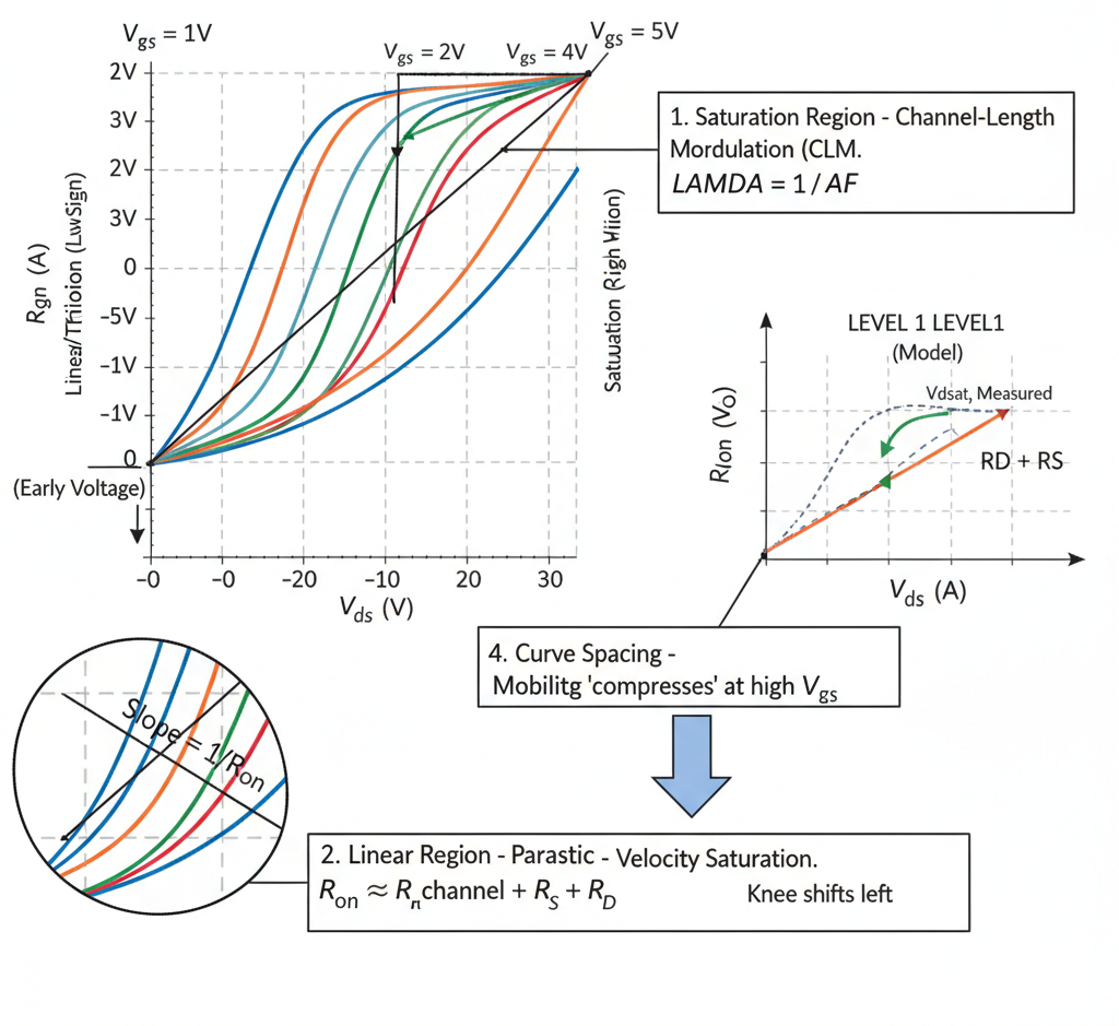
Fig. 1. MOSFET Output Characteristics: Parameter Extraction
Introduction
The output characteristic plot ($I_d$ vs. $V_d$) is a fundamental MOSFET measurement. It shows how the drain current ($I_d$) varies with the drain-source voltage ($V_{ds}$), for several different constant gate-source voltages ($V_{gs}$).
This family of curves is essential for extracting parameters that model the transistor's behavior in the linear (or triode) region and the saturation region.
The plot is typically divided into two main regions:
- Linear/Triode Region (Low $V_{ds}$): The device acts like a voltage-controlled resistor. $I_d$ rises linearly (or near-linearly) with $V_{ds}$.
- Saturation Region (High $V_{ds}$): The channel "pinches off," and the device acts like a voltage-controlled current source. Ideally, $I_d$ would be constant, but real-world effects cause it to slope upwards.
1. Saturation Region - Channel-Length Modulation (LEVEL 1, 2, 3)
In the simple (LEVEL 1) model, the saturation current is assumed to be constant and independent of $V_{ds}$. In reality, the $I_d$ curves slope gently upwards.
Physical Cause: This is due to Channel-Length Modulation (CLM), an effect analogous to the Early effect in BJTs. As $V_{ds}$ increases, the depletion region at the drain end of the channel widens, which moves the "pinch-off" point slightly toward the source. This reduces the effective channel length ($L_{eff}$). Since $I_d$ is inversely proportional to $L_{eff}$, the current increases slightly.
SPICE Parameter:
LAMBDA(Channel-Length Modulation Parameter)- The LEVEL 1 model modifies the saturation current: $$I_d = I_{d,sat} \cdot (1 + \lambda \cdot V_{ds})$$
Extraction Method:
- For each $I_d$ curve (at a constant $V_{gs}$), draw a straight-line tangent along the sloped portion in the saturation region.
- Extrapolate all these tangent lines backward. They will ideally converge at a single point on the negative $V_{ds}$ axis.
- This intercept is the Early Voltage ($VAF$ or $V_A$).
- The
LAMBDAparameter is the inverse of the Early Voltage: $$\lambda = \frac{1}{VAF}$$
2. Linear Region - Parasitic Resistances (LEVEL 3, 6)
The simple LEVEL 1 model assumes the "on-resistance" ($R_{on}$) at very low $V_{ds}$ is determined only by the ideal channel. In reality, parasitic resistances from the source and drain contacts/regions add to this.
- Physical Cause: There is a physical, ohmic resistance in the source and drain regions ($R_s$ and $R_d$) that is in series with the ideal MOSFET channel.
- SPICE Parameters:
RD(Drain Resistance),RS(Source Resistance) - Effect on Plot: These resistances "linearize" the $I_d-V_d$ curve near the origin. The slope of the curve at $V_{ds} \approx 0$ is the total on-resistance ($R_{on}$). $$R_{on} = \frac{V_{ds}}{I_d} = R_{channel} + RD + RS$$
- Extraction Method:
- Measure $R_{on}$ (the slope near the origin) for several different, high $V_{gs}$ values.
- The channel resistance ($R_{channel}$) decreases as $V_{gs}$ increases, while
RDandRSare constant. - By plotting $R_{on}$ (y-axis) vs. a function of the gate voltage (e.g., $1/(V_{gs} - VTO)$) (x-axis), a straight line is obtained.
- The y-intercept of this plot (where the channel resistance term goes to zero) gives the sum of the parasitic resistances,
RD + RS. - (Separate
RDandRSrequires more advanced "Kelvin" measurement structures).
3. Saturation Knee - Velocity Saturation (LEVEL 2, 6)
For short-channel devices, the simple "pinch-off" model (LEVEL 1) breaks down. Carriers reach a maximum speed before the channel pinches off.
- Physical Cause: At high electric fields (high $V_{ds}$ over a short $L$), the charge carriers (electrons or holes) reach a maximum scatter-limited velocity and cannot travel any faster.
- SPICE Parameter:
VMAX(Maximum Drift Velocity) - Effect on Plot:
- The "knee" of the curve (transition from linear to saturation) occurs at a lower $V_{ds}$ than LEVEL 1 predicts.
- The saturated $I_d$ becomes more proportional to $(V_{gs} - VTO)$ instead of $(V_{gs} - VTO)^2$.
- Extraction Method:
VMAXis a physical parameter that is difficult to extract with a simple graphical method. It is primarily a fitting parameter. In LEVEL 2 or LEVEL 6 (BSIM),VMAXis adjusted in the model until the "knee" of the output curve and the resulting saturation current level match the measured data, especially at high $V_{gs}$.
4. Curve Spacing - Mobility Degradation (LEVEL 3, 6)
The output plot also clearly visualizes the effect of mobility degradation, even though the parameters are typically extracted from the $I_d$ vs. $V_g$ transfer plot.
- Physical Cause: At high $V_{gs}$ values, the strong vertical electric field pulls carriers against the silicon-oxide interface. This increases scattering and reduces their mobility.
- SPICE Parameters:
THETA(LEVEL 3),U0,UA,UB... (LEVEL 6/BSIM) - Effect on Plot: The vertical spacing between $I_d$ curves (for constant $V_{gs}$ steps) is not constant. At high $V_{gs}$ levels, this spacing "compresses" or gets smaller, indicating a loss of "gain" (transconductance).
- Extraction: These parameters are adjusted using numerical optimization to fit this observed current compression in the high-$V_{gs}$ region of the plot.