
Latch and Flip-Flops
RS Flip-Flop
Circuit Diagram
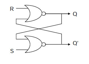
Figure 1: Basic RS Flip-Flop circuit diagram using two cross-coupled NOR gates. Reference: Theory section
Components Available in Simulation
- Pre-built RS Flip-Flop component
- Input sources (S, R, CLK)
- Output displays (Q, Q')
Simulation Instructions
- Select RS Flip-Flop tab in the simulation interface.
- Observe the pre-built RS Flip-Flop component displayed in the working area.
- Set input values for S (Set) and R (Reset) using the input controls.
- Toggle the clock signal if available to observe synchronous behavior.
- Observe the outputs Q and Q' and verify they follow the RS flip-flop truth table.
- Test different input combinations:
- S=0, R=0: Hold state
- S=1, R=0: Set (Q=1)
- S=0, R=1: Reset (Q=0)
- S=1, R=1: Invalid state (avoid this)
- Click "Simulate" to run the simulation and observe the behavior.
Learning Objectives
- Understand RS flip-flop operation through interactive simulation
- Observe the relationship between inputs (S, R) and outputs (Q, Q')
- Learn about the invalid state condition
- Visualize the memory function of flip-flops
D Flip-Flop
Circuit Diagram
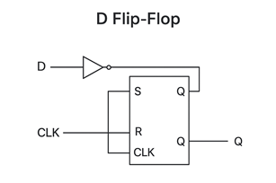
Figure 2: D Flip-Flop circuit diagram showing data input with clock control for synchronous operation. Reference: Theory section
Components Available in Simulation
- Pre-built D Flip-Flop component
- Input sources (D, CLK)
- Output displays (Q, Q')
Simulation Instructions
- Select D Flip-Flop tab in the simulation interface.
- Observe the pre-built D Flip-Flop component displayed in the working area.
- Set the D input value using the input control (0 or 1).
- Apply clock pulses using the clock control to trigger the flip-flop.
- Observe the outputs Q and Q' after each clock edge.
- Verify the operation:
- On positive clock edge: Q becomes equal to D
- Between clock edges: Q remains stable regardless of D changes
- Test with different sequences:
- Set D=1, apply clock → Q should become 1
- Set D=0, apply clock → Q should become 0
- Change D without clock → Q should remain unchanged
- Click "Simulate" to run the simulation animation.
Learning Objectives
- Understand edge-triggered operation of D flip-flops
- Observe data transfer from input to output on clock edges
- Learn about synchronous digital system behavior
- Visualize how D flip-flops eliminate invalid states
JK Flip-Flop
Circuit Diagram
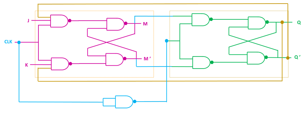
Figure 3: Master-Slave JK Flip-Flop circuit diagram showing master and slave latches for race-condition elimination. Reference: Theory section
Components Available in Simulation
- Pre-built JK Flip-Flop component
- Input sources (J, K, CLK)
- Output displays (Q, Q')
Simulation Instructions
- Select JK Flip-Flop tab in the simulation interface.
- Observe the pre-built JK Flip-Flop component displayed in the working area.
- Set input values for J and K using the input controls.
- Apply clock pulses using the clock control to trigger the flip-flop.
- Observe the outputs Q and Q' after each clock edge.
- Test all four operations:
- Hold: J=0, K=0 → Q remains unchanged
- Set: J=1, K=0 → Q becomes 1
- Reset: J=0, K=1 → Q becomes 0
- Toggle: J=1, K=1 → Q changes to its complement
- Verify edge-triggered behavior: Changes occur only on clock transitions.
- Click "Simulate" to run the simulation animation.
Learning Objectives
- Understand the versatility of JK flip-flops (all four operations)
- Observe how JK flip-flops eliminate the invalid state problem
- Learn about toggle operation for counter applications
- Visualize master-slave operation preventing race conditions
T Flip-Flop
Circuit Diagram
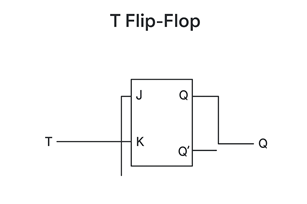
Figure 4: T Flip-Flop circuit diagram implemented using JK Flip-Flop with J and K inputs tied together. Reference: Theory section
Components Available in Simulation
- Pre-built T Flip-Flop component
- Input sources (T, CLK)
- Output displays (Q, Q')
Simulation Instructions
- Select T Flip-Flop tab in the simulation interface.
- Observe the pre-built T Flip-Flop component displayed in the working area.
- Set the T input value using the input control (0 or 1).
- Apply clock pulses using the clock control to trigger the flip-flop.
- Observe the outputs Q and Q' after each clock edge.
- Test both operations:
- Hold: T=0 → Q remains unchanged after clock edge
- Toggle: T=1 → Q changes to its complement after clock edge
- Observe frequency division: When T=1, output frequency is half the clock frequency.
- Click "Simulate" to run the simulation animation.
Learning Objectives
- Understand toggle operation and its applications
- Observe frequency division property (output = clock ÷ 2)
- Learn how T flip-flops are used in counters
- Visualize the relationship between T flip-flops and JK flip-flops
General Simulation Tips
Navigation
- Tab Selection: Click on the tabs (RS Flip-Flop, D Flip-Flop, JK Flip-Flop, T Flip-Flop) to switch between different flip-flop demonstrations.
- Input Controls: Use the provided input controls to set values for inputs like S, R, D, J, K, T.
- Clock Control: Use the clock control to apply clock pulses and observe edge-triggered behavior.
Simulation Features
- Visual Animation: Each simulation provides visual animations showing the flip-flop operation.
- Real-time Output: Observe how outputs change in response to input changes and clock edges.
- Interactive Learning: Experiment with different input combinations to understand flip-flop behavior.
Learning Approach
- Start with RS Flip-Flop: Understand basic latch operation and memory function.
- Progress to D Flip-Flop: Learn about edge-triggered operation and data storage.
- Explore JK Flip-Flop: Understand the versatile four-operation capability.
- Finish with T Flip-Flop: Learn about toggle operation and frequency division.
Troubleshooting
- No Animation: Ensure you've clicked the "Simulate" button after setting inputs.
- Unexpected Output: Verify input settings and check if you're applying clock edges correctly.
- Interface Issues: Try refreshing the page if the simulation interface becomes unresponsive.