
Voltage Current Characteristics of Insulated Gate Bipolar Transistor (IGBT)
Introduction
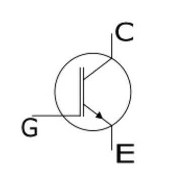
The Insulated Gate Bipolar Transistor (IGBT) is a semiconductor device having three terminals – Gate (G), Emitter (E), and Collector (C) and is used mainly as an electronic switch. It is characterized by fast switching and high efficiency, which makes it a necessary component in modern appliances such as lamp ballasts, electric cars and variable frequency drives VFDs. Its ability to turn on and off, rapidly, makes it applicable in amplifiers to process complex wave-patterns with pulse width modulation. IGBT combines the characteristics of MOSFETs and BJTs to attain high current and low saturation voltage capacity respectively. It integrates an isolated gate using FET Field effect transistor to obtain a control input.
IGBT is also known as Insulated Gate Transistor (IGT), Metal Oxide Insulated Gate Transistor (MOSIGT), Conductively Modulated Field Effect Transistor (COMFET) or Gain Modulated FET (GEMFET).
Basic Structure And Working Of IGBT
The IGBT is constructed by a p+ layer substrate from the collector. In the IGBT, the p+ substrate is called the injection layer since it injects holes into the N- layer (in between the P+ layer and P layer) is called drift region. The thickness of N- layer determines the voltage blocking capability of the IGBT. The P-layer is known as the body region of the IGBT and the body region serves to accommodate depletion of junction J2.
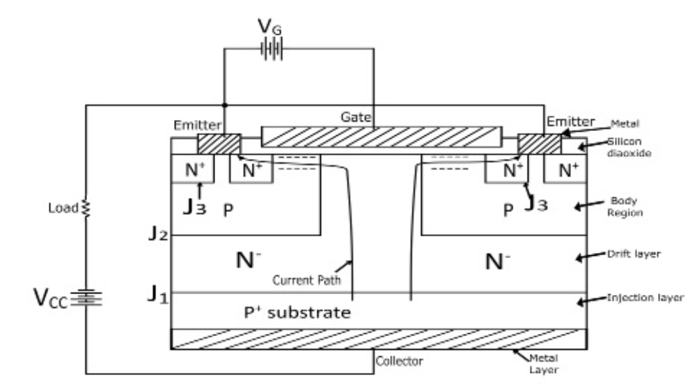
When collector is made positive with respect to the emitter, the IGBT is forward biased. When voltage is not applied between gate and emitter, the junction J2 between N- region and P region is reverse biased, hence no current flows from collector to emitter.
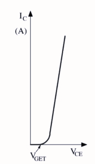
When gate is applied with positive voltage with respect to emitter by source VG, with gate-emitter voltage greater than threshold voltage (VGET) of the IGBT, then n-channel or inversion layer is induced in the upper part of p-region just below the gate. This n-channel short circuits the N--region with the N+-emitter regions.
Electrons start to flow from N+ region to N- region through the n-channel. Since the IGBT is forward biased, hence the P+ collector region injects holes into the N- drift region, so that the injection carrier density in the N- drift region increases extensively and in turn, the conductivity of N- region increases significantly. Hence the IGBT gets turned ON and starts to conduct forward collector current IC.
The collector current (IC) or emitter current (IE) consists of two components viz. one is Hole Current (Ih) due to the injected holes and another is Electron Current (Ie) due to injected electrons.
IGBT Characteristics
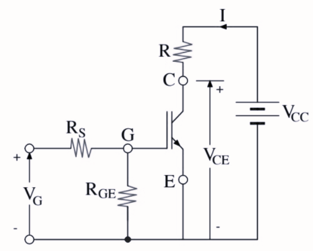
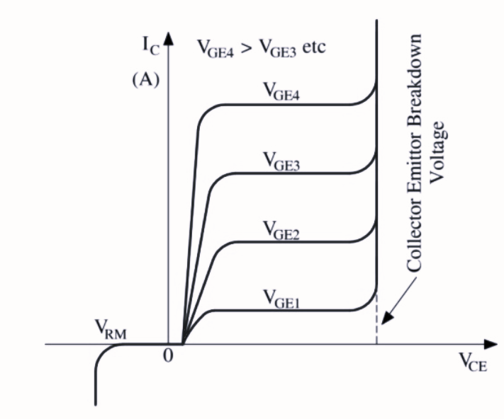
The gate-emitter voltage (VGE) is varied and the collector-emitter voltage (VCE) and collector current (IC) is measured. Then a plot between IC & VCE is drawn. This plot is the required static characteristics of IGBT. When the device is forward biased, the shape of output characteristics is similar to that of BJT. However, the controlling parameter in case of IGBT is VGE as it is a voltage-controlled device. When the device is reversed biased, there is a voltage beyond which breakdown occurs. This reverse voltage is shown to be VRM. There is a maximum voltage in forward conduction mode beyond which collector-emitter breakdown occurs and gate losses control of collector current.
Transfer Characteristics
The transfer characteristics of IGBT is basically a plot of collector current IC versus gate-emitter voltage (VGE).
Advantages of IGBT
IGBTs can handle high voltages and currents, making them suitable for high-power applications such as motor drives, power inverters, and industrial equipment.
IGBTs have a low voltage drop across the device when it is conducting, resulting in reduced power dissipation and higher efficiency.
IGBTs have faster switching speeds compared to traditional power BJTs, which enables them to operate at higher frequencies and reduces switching losses.
IGBTs have a voltage-controlled gate, like a MOSFET, which requires less current to drive the gate compared to a BJT. This simplifies the gate drive circuitry and control requirements.
IGBTs typically have low on-resistance, leading to lower conduction losses and higher efficiency in power applications.
IGBTs have a rugged structure that allows them to withstand high voltage and current stresses, making them reliable and suitable for demanding applications.
IGBTs have inherent short-circuit protection due to their positive temperature coefficient characteristics, which helps prevent catastrophic failures under fault conditions.
IGBTs are available in a wide range of voltage and current ratings, providing flexibility in designing various power electronics applications.
Since IGBTs require relatively low gate drive power compared to other power devices, the overall system complexity and power losses are reduced.
Disadvantages of IGBT
IGBTs have higher switching losses compared to other power semiconductor devices, such as MOSFETs. These losses occur during the transition between the on and off states, leading to power dissipation and reduced efficiency.
IGBTs are not well-suited for high-frequency applications due to their relatively slow switching speed. This limitation makes them less suitable for high-frequency switching power converters and other high-frequency circuits.
IGBTs can generate a significant amount of heat during operation, especially in high-power applications. Proper cooling and thermal management are essential to prevent overheating and ensure the reliability of the device.
IGBTs require complex drive circuits to control their gate voltage and current during switching. This complexity can increase the cost and design challenges in some applications.
While IGBTs are available in various voltage and current ratings, their limitations may not always meet the requirements of extremely high-power applications.
In high-voltage applications, IGBTs may experience issues with voltage spikes and surges, leading to the risk of breakdown and failure.
Applications of IGBT
IGBT are used in dc and ac motor drives.
Used in UPS systems.
Used in power supplies and drivers for solenoids, relays and contactors.
Used in Medical Equipment.
IGBT are also used in Robotics and Automation.