
Performance Measurement and Analysis of Non-isolated DC-DC Boost Converter
Theory
The circuit configuration of boost converter is given in Fig. 1
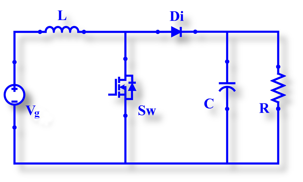
Fig. 1 Circuit configuration of Boost Converter.
Based on the operation of switch (Sw: ON/OFF-state) the operating principle of the converter is explained below briefly.
|
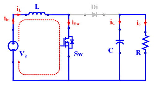
Mode – I : Switch (Sw): ON and Diode (Di): OFF
|
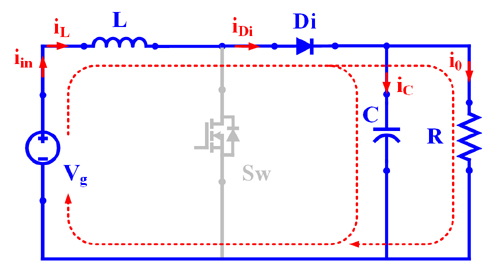
Mode – II : Switch (Sw): OFF and Diode (Di): ON
|
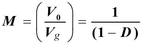
a) Voltage conversion ratio or voltage gain (M)
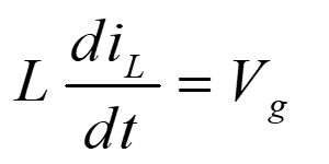
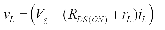
Voltage across inductor L:
Mode – I :

Mode – II :

Applying volt-sec balance on inductor (eqn. 1 and 2)

On simplifying the eqn. 3
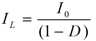
b) Average current through inductor (IL):
Current through capacitor
Mode – I :
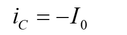
Mode – II :
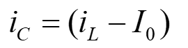
Applying charge-sec balance on capacitor (eqn. 5 and 6)
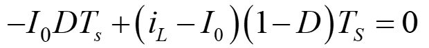
On solving eqn. 7
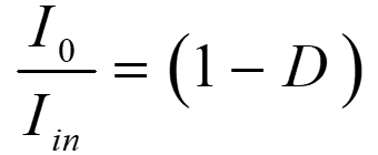
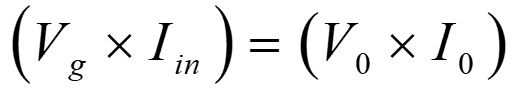
c) Power balance under ideal condition (neglecting losses):
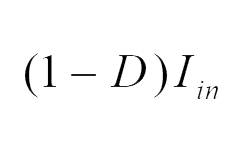
From Fig. 1, the source current itself is the inductor current and hence
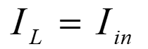
Simplifying eqns. 8 and 9 gives the current gain
From eqns. 4 and 10
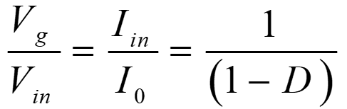
Hence under ideal condition, the power drawn from the source is equal to power supplied to load.
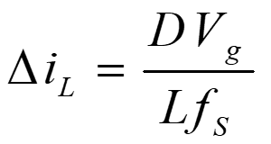
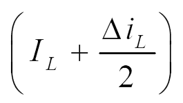
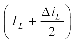
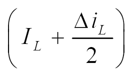
d) Inductor current ripple:
From eqn. 1,
Therefore, the inductor ripple current is
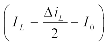
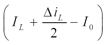
e) Current through various components:
The current through various components are given in Fig. 3.
Fig. 3. Current through various components.
|
Mode-I (DT) |
Mode-II (1-D)T |
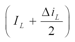
Average Current | |||
| imin | imax | imin | imax | Iavg | |
| iL | 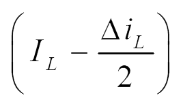 |
 |
 |
 |
 |
| iC |  |
 |
 |
 |
0 |
| iSw |  |
 |
0 | 0 | 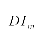 |
| iDi | 0 | 0 | 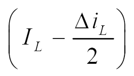 |
 |
 |
f) Voltage and current stress on various components:
| Component | Voltage stress | Current Stress |
| Inductor (L) | 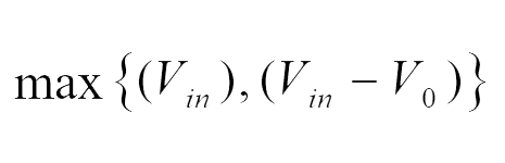 |
 |
| Capacitor (C) | V0 | 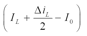 |
| Switch (Sw) | V0 |  |
| Diode (Di) | V0 | 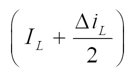 |
g) Efficiency analysis:

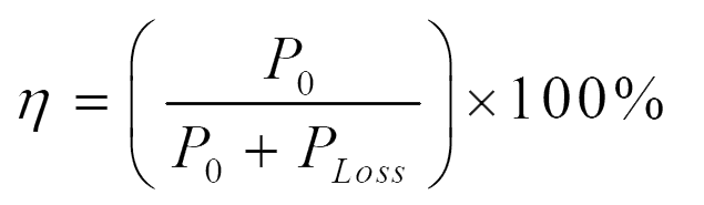
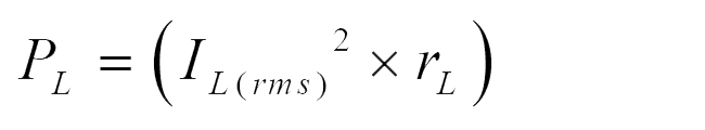
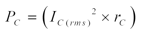
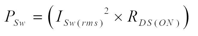
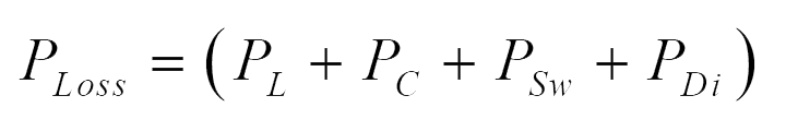
The power loss occurring in various components are given below.
Power loss in inductor:
Power loss in capacitor:
Power loss in switch:
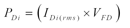
Power loss in Diode:
Total power loss:
h) Effect of non-idealities on voltage gain expression:
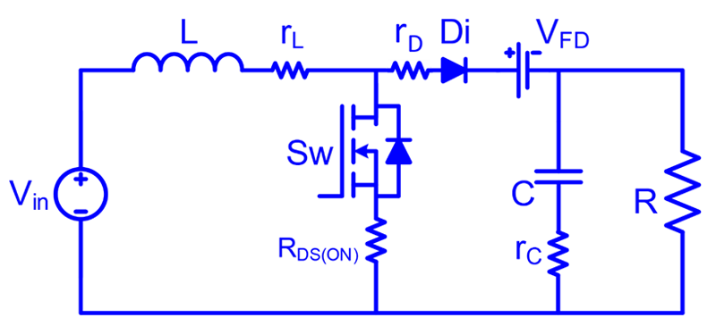
Fig. 4. Circuit configuration of conventional boost converter with non-idealities.
Based on the operation of switch (Sw: ON/OFF-state) the operating principle of the converter is explained below briefly.
Voltage across inductor L
Mode – I :
Mode – II :

Applying volt-sec balance on inductor (eqn. 22 and 23)

Therefore, voltage gain of non-ideal boost converter is