
Multipliers
2-Bit Binary Multiplier
Circuit Diagram
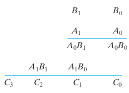
Figure 1: 2-bit multiplier circuit diagram using AND gates for partial product generation and half adders for summation. Reference: Theory section
Components Required
- 4 AND gates
- 2 Half adders
Circuit Connections
- Drag the first AND gate and connect its inputs to A₀ and B₀. This generates partial product P₀₀.
- Drag the second AND gate and connect its inputs to A₀ and B₁. This generates partial product P₀₁.
- Drag the third AND gate and connect its inputs to A₁ and B₀. This generates partial product P₁₀.
- Drag the fourth AND gate and connect its inputs to A₁ and B₁. This generates partial product P₁₁.
- Drag the first Half Adder (HA₁) and connect its inputs to the outputs of the second AND gate (P₀₁) and third AND gate (P₁₀).
- Connect the Sum output of HA₁ to output bit C₁.
- Drag the second Half Adder (HA₂) and connect its inputs to the Carry output of HA₁ and the output of the fourth AND gate (P₁₁).
- Connect the Sum output of HA₂ to output bit C₂.
- Connect the Carry output of HA₂ to output bit C₃.
- Connect the output of the first AND gate (P₀₀) directly to output bit C₀.
- Set the input values for A₁, A₀, B₁, B₀ and click "Simulate".
Observations
- The output C₃C₂C₁C₀ represents the 4-bit product of the 2-bit multiplicand (A₁A₀) and 2-bit multiplier (B₁B₀).
- For example: If A₁A₀ = 11₂ (3₁₀) and B₁B₀ = 10₂ (2₁₀), then C₃C₂C₁C₀ = 0110₂ (6₁₀).
- If the circuit has been constructed as described above, a "Success" message will be displayed upon clicking "Submit".
4-Bit Array Multiplier
Circuit Diagram
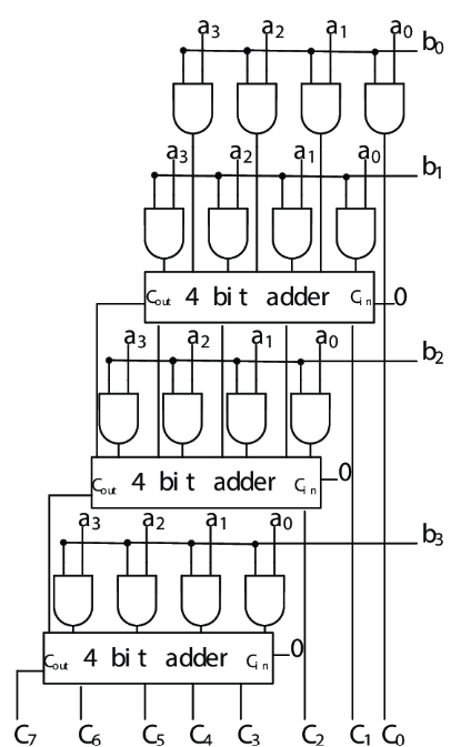
Figure 2: 4-bit array multiplier circuit diagram showing systematic partial product generation and addition stages. Reference: Theory section
Components Required
- 16 AND gates (for 4×4 partial product matrix)
- Multiple Half adders and Full adders for partial product summation
- Proper carry propagation connections
Circuit Connections
- Create the first row of partial products by dragging 4 AND gates and connecting them as follows:
- First AND gate: inputs A₀ and B₀ (generates P₀₀)
- Second AND gate: inputs A₀ and B₁ (generates P₀₁)
- Third AND gate: inputs A₀ and B₂ (generates P₀₂)
- Fourth AND gate: inputs A₀ and B₃ (generates P₀₃)
- Create the second row of partial products by dragging 4 AND gates and connecting them as follows:
- Fifth AND gate: inputs A₁ and B₀ (generates P₁₀)
- Sixth AND gate: inputs A₁ and B₁ (generates P₁₁)
- Seventh AND gate: inputs A₁ and B₂ (generates P₁₂)
- Eighth AND gate: inputs A₁ and B₃ (generates P₁₃)
- Create the third row of partial products by dragging 4 AND gates and connecting them as follows:
- Ninth AND gate: inputs A₂ and B₀ (generates P₂₀)
- Tenth AND gate: inputs A₂ and B₁ (generates P₂₁)
- Eleventh AND gate: inputs A₂ and B₂ (generates P₂₂)
- Twelfth AND gate: inputs A₂ and B₃ (generates P₂₃)
- Create the fourth row of partial products by dragging 4 AND gates and connecting them as follows:
- Thirteenth AND gate: inputs A₃ and B₀ (generates P₃₀)
- Fourteenth AND gate: inputs A₃ and B₁ (generates P₃₁)
- Fifteenth AND gate: inputs A₃ and B₂ (generates P₃₂)
- Sixteenth AND gate: inputs A₃ and B₃ (generates P₃₃)
- Connect P₀₀ directly to output bit P₀.
- Use Half Adders and Full Adders to sum the partial products column-wise:
- Column 1: Use Half Adder to add P₀₁ and P₁₀, connect Sum to P₁ and Carry to next stage
- Column 2: Use Full Adder to add P₀₂, P₁₁, and carry from column 1, connect appropriately
- Continue this pattern for remaining columns, ensuring proper carry propagation
- Connect the final outputs to P₇P₆P₅P₄P₃P₂P₁P₀.
- Set the input values for A₃A₂A₁A₀ and B₃B₂B₁B₀, then click "Simulate".
Observations
- The output P₇P₆P₅P₄P₃P₂P₁P₀ represents the 8-bit product of two 4-bit numbers.
- Maximum product: 15 × 15 = 225 = 11100001₂
- The array multiplier provides a systematic approach to binary multiplication with predictable timing.
- If the circuit has been constructed correctly with proper carry connections, a "Success" message will be displayed upon clicking "Submit".
4-Bit Advanced Multiplier
Circuit Diagram
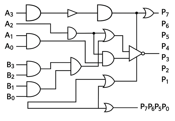
Figure 3: 4-bit advanced multiplier circuit diagram showing optimized implementation with additional logic gates. Reference: Theory section
Components Required
- 16 AND gates (for partial product generation)
- Multiple Half adders and Full adders
- NOT gates for signal inversion and optimization
- XOR and OR gates for enhanced logic operations
Circuit Connections
- Follow the same partial product generation steps as the 4-Bit Array Multiplier (steps 1-4 above).
- Implement optimized addition network using available logic gates:
- Use NOT gates for signal inversion where beneficial
- Employ XOR gates for sum generation in custom adder configurations
- Utilize OR gates for optimized carry generation
- Connect the addition network with proper carry propagation, taking advantage of the extended gate library for optimization.
- Ensure all partial products are properly summed and connected to output bits P₇P₆P₅P₄P₃P₂P₁P₀.
- Set the input values for A₃A₂A₁A₀ and B₃B₂B₁B₀, then click "Simulate".
Observations
- The circuit demonstrates advanced multiplier design techniques with optimized logic.
- Output P₇P₆P₅P₄P₃P₂P₁P₀ represents the same 8-bit product but with potentially improved characteristics.
- Students can explore different optimization strategies using the available gate library.
- If the circuit has been constructed correctly, a "Success" message will be displayed upon clicking "Submit".
Wallace Tree Multiplier
Circuit Diagram
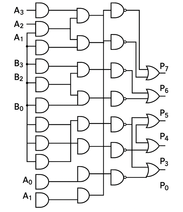
Figure 4: Wallace tree multiplier circuit diagram showing parallel reduction tree structure for high-speed multiplication. Reference: Theory section
Components Required
- 16 AND gates (for partial product generation)
- Multiple Half adders and Full adders arranged in tree structure
- Complete logic gate library (AND, OR, XOR, NOT, NAND, NOR) for optimization
- Proper tree-structured carry-save addition network
Circuit Connections
- Generate all 16 partial products using AND gates as in previous implementations (steps 1-4 from 4-Bit Array Multiplier).
- Implement Wallace tree reduction:
- Group partial products into sets of three and use Full Adders for 3:2 compression
- Group remaining pairs and use Half Adders for 2:2 compression
- Continue reduction stages until only two operands remain
- Use the complete gate library for optimization:
- NAND gates can replace AND-NOT combinations for area efficiency
- NOR gates can replace OR-NOT combinations
- Implement custom logic using universal gates where beneficial
- Implement final ripple carry adder or carry lookahead adder for the last two operands.
- Connect the final outputs to P₇P₆P₅P₄P₃P₂P₁P₀.
- Set the input values for A₃A₂A₁A₀ and B₃B₂B₁B₀, then click "Simulate".
Observations
- The Wallace tree structure minimizes the critical path delay through parallel processing.
- Output P₇P₆P₅P₄P₃P₂P₁P₀ represents the 8-bit product with optimized timing characteristics.
- The tree structure trades area for speed, demonstrating important design trade-offs.
- Advanced students can explore different tree configurations and optimization techniques.
- If the circuit has been constructed correctly with proper tree structure, a "Success" message will be displayed upon clicking "Submit".