
Extraction of MOSFET LEVEL (1,2,3 and 6) SPICE parameters related to gate voltage Capacitance (Cg vs. Vg) 
Theory
Introduction:
MOSFET C-V Parameter Extraction (Cg vs. Vg)
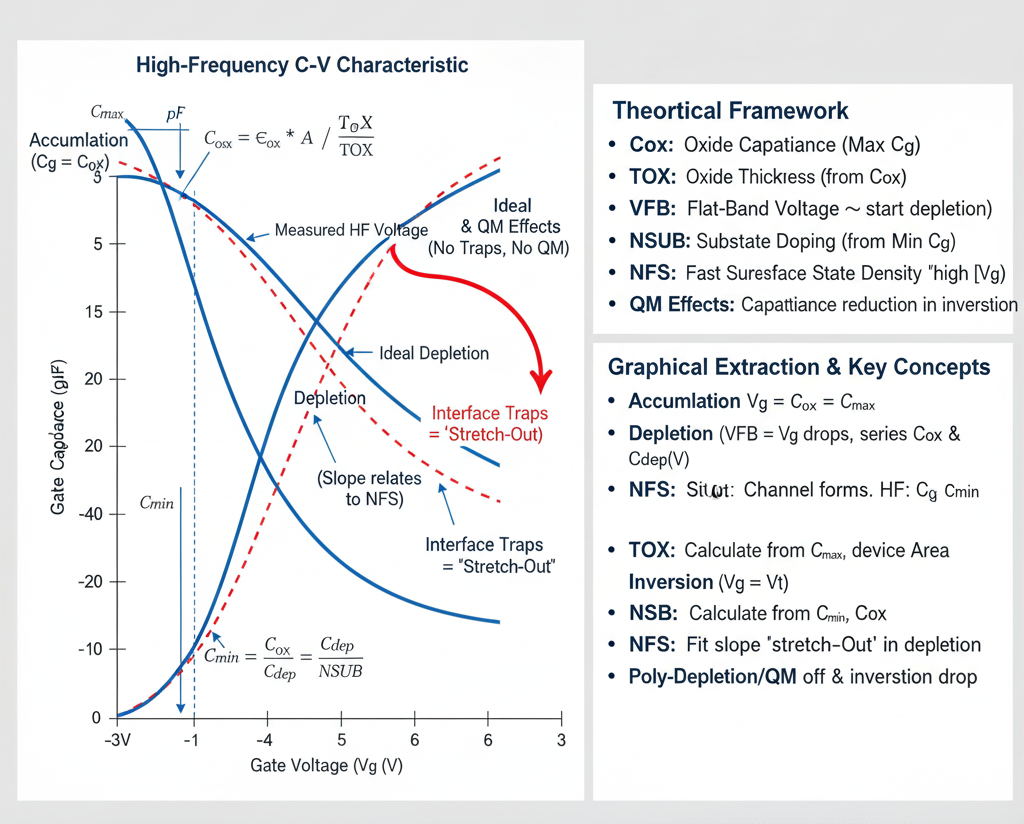
Fig. 1. MOSFET Cg vs Vg Capacitance-Voltage Characteristics & SPICE Parameter Extraction
Introduction
The Gate Capacitance versus Gate Voltage (Cg vs. Vg) measurement is one of the most powerful methods for extracting a MOSFET's physical parameters. It involves measuring the capacitance of the MOS "stack" (Gate-Oxide-Substrate) as the gate voltage ($V_g$) is swept, while the source, drain, and bulk are typically grounded.
The C-V curve has three distinct regions, which are fundamental to understanding the device and its parameters:
- Accumulation (Negative $V_g$ for NMOS): The gate voltage attracts majority carriers (holes) to the silicon-oxide interface. The device acts like a simple parallel-plate capacitor, and the measured capacitance is at its maximum, $C_{max}$.
- Depletion (Small Positive $V_g$ for NMOS): The gate voltage pushes majority carriers away, leaving a "depletion region" of fixed ions. This depletion region has its own capacitance ($C_{dep}$) which acts in series with the oxide capacitance ($C_{ox}$). This causes the total capacitance to drop.
- Inversion (High Positive $V_g$ for NMOS, $V_g > V_t$): The gate voltage is strong enough to attract minority carriers (electrons), forming the inversion layer, or "channel."
High-Frequency vs. Low-Frequency C-V
- Low-Frequency (LF): The AC signal is slow enough that the minority carriers in the channel can respond. The channel effectively acts as the bottom "plate" of the capacitor, and the capacitance returns to its maximum value, $C_{ox}$.
- High-Frequency (HF): (e.g., 1 MHz). The AC signal is too fast for the minority carriers to be generated and respond. The AC signal only "sees" the underlying depletion region, which is at its maximum width. Therefore, the capacitance stays at its minimum value ($C_{min}$).
SPICE parameter extraction is almost always performed using the High-Frequency (HF) C-V curve.
1. Oxide and Substrate Parameters (LEVEL 1, 2, 3)
TOX (Oxide Thickness)
- Theory: The maximum capacitance ($C_{max}$) measured in the strong accumulation region is equal to the oxide capacitance ($C_{ox}$). $$C_{max} = C_{ox} = \frac{\epsilon_{ox} \cdot A}{TOX}$$
- Extraction:
- Measure $C_{max}$ from the "high" plateau of the C-V curve.
- Knowing the device area ($A$) and the permittivity of silicon dioxide ($\epsilon_{ox}$),
TOXcan be directly calculated. - This is the most important parameter, as
TOX(or $C_{ox}$) is used in the equations for almost all other parameters (likeKP,GAMMA, etc.).
NSUB (Substrate Doping)
- Theory: The minimum capacitance ($C_{min}$) on the HF C-V plot occurs when the depletion region is at its maximum width ($W_{d,max}$). This minimum capacitance is $C_{ox}$ in series with the maximum depletion capacitance ($C_{dep,max}$).
$$C_{min} = \frac{C_{ox} \cdot C_{dep,max}}{C_{ox} + C_{dep,max}}$$
The maximum depletion width ($W_{d,max}$) is physically determined by the substrate doping concentration,
NSUB. - Extraction:
- Measure $C_{min}$ from the "low" plateau of the C-V curve.
- Using the $C_{ox}$ value found from $C_{max}$, solve the series-capacitor equation to find $C_{dep,max}$.
- From $C_{dep,max}$, the underlying physical parameter
NSUBcan be calculated.
VFB (Flat-Band Voltage)
- Theory: This is the gate voltage required to counteract the work-function differences and fixed oxide charges (
Qf), resulting in "flat" energy bands in the silicon. It is the theoretical transition point between accumulation and depletion. - Extraction:
VFBis not a simple intercept. It is extracted by analyzing the "shoulder" of the C-V curve as it transitions from $C_{max}$ into depletion. Advanced calculation methods (like finding the inflection point or using a "flat-band capacitance" value) are used to pinpointVFB.
2. Interface Effects (LEVEL 3)
NFS (Fast Surface States / Interface Traps)
- Theory: Real Si/SiO2 interfaces have "traps" (defects) that can capture or release charge. As the gate voltage sweeps through depletion, these traps must be charged/discharged, which also consumes part of the AC signal.
- Effect on Plot: This "wastes" charge and makes the C-V curve "stretch out," meaning the slope in the depletion region becomes less steep than the ideal curve.
- Extraction:
NFSis a fitting parameter. The slope of the measured C-V curve in the depletion region is compared to the ideal slope (calculated fromTOXandNSUB). The amount of "stretch-out" is used to quantify and extractNFS.
3. Advanced Physical Effects (LEVEL 6 - BSIM)
For modern devices, two advanced effects (which are not modeled in LEVEL 1-3) must be accounted for.
Polysilicon Gate Depletion
- Theory: The polysilicon gate is not a perfect metal. At high positive or negative gate voltages, a depletion region forms in the polysilicon gate itself. This poly-depletion layer has its own capacitance ($C_{poly}$) that is in series with $C_{ox}$.
- Effect on Plot: This causes a roll-off or decrease in the measured capacitance in the strong accumulation and inversion (LF) regions. The measured "maximum" capacitance is slightly lower than the true $C_{ox}$.
- Extraction: This is a fitting parameter in advanced models. The model is adjusted until it correctly fits this roll-off at high gate voltages.
Quantum Mechanical (QM) Effects
- Theory: In strong inversion, the channel (inversion layer) is not a 2D sheet sitting perfectly at the Si/SiO2 interface. Quantum mechanics confines the electrons to a region slightly away from the interface.
- Effect on Plot: This physical separation acts like a small, extra capacitor ($C_{qm}$) in series with $C_{ox}$. This lowers the total measured capacitance in the inversion region, even on an LF plot.
- Extraction: This is another advanced fitting parameter. The model equations are adjusted until they match the measured capacitance reduction in the strong inversion region.