C-V characterization of PMOS capacitors 
Procedure

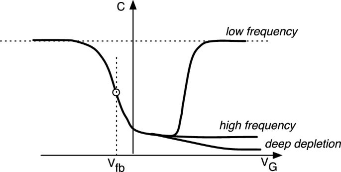
Fig. 1. MOS C/V curve
- Set Material Parameters:
- Choose the semiconductor material (Si, Ge, GaAs) for the simulation by clicking on the respective button.
- Enter the work function of the metal gate, ϕm, in electron volts (eV).
- Input the electron affinity of the semiconductor, χs, in eV.
- Define Oxide Properties:
- Enter the oxide thickness, tox, in nanometers (nm).
- Specify the relative permittivity of the oxide, εox.
- Set Semiconductor Parameters:
- Specify the relative permittivity of the semiconductor, εsemi.
- Enter the effective density of states in the conduction band, Nc, and in the valence band, Nv, in 1/cm3.
- Set the temperature, T, in Kelvin (K).
- Input the acceptor doping concentration, NA, in 1/cm3.
- Calculate Energy Bandgap:
- Use the given formula to calculate the energy bandgap, Eg, based on the temperature.
- Submit the Parameters:
- Click the "Submit" button to apply the parameters and perform the simulation.
- Analyze the Results:
- Observe the Q-V (Charge-Voltage) and C-V (Capacitance-Voltage) plots generated from the simulation.
- Examine key parameters displayed, such as oxide capacitance (Cox), threshold voltage (VT), flat-band voltage (Vfb), and others.
- Interpret the different regions in the C-V curve: accumulation, depletion, and inversion, to understand the behavior of the PMOS capacitor.
