Performance measurement and analysis of DC-DC boost regulator
Theory
The circuit configuration of boost converter is given in Fig. 1.
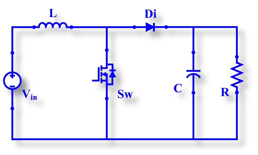
Fig. 1 Circuit Diagram of Boost Converter.
Based on the modes of operation, the voltage gain formulation (in brief) is given below:
|
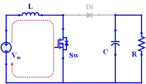
Mode – I : Switch S:ON-state, Diode: OFF-state
|
Mode – II : Switch S:OFF-state, Diode: ON-state
|

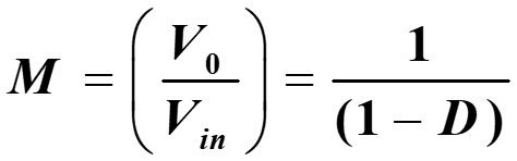
a) Voltage conversion ratio or voltage gain (M)
Voltage across inductor L:
Mode – I :

Mode – II :

Applying volt-sec balance on inductor (eqn. 1 and 2)

On simplifying the eqn. 3
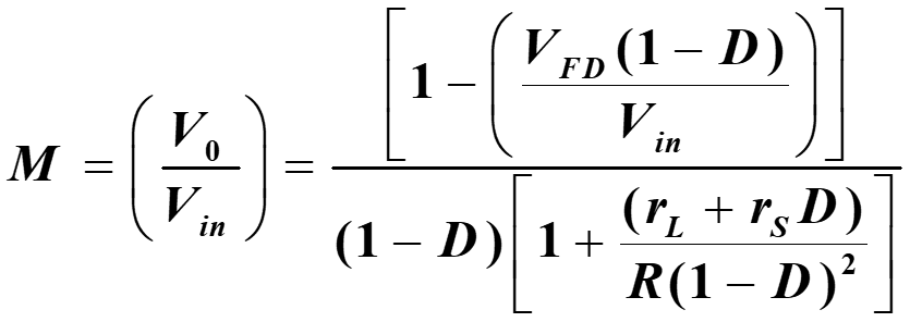
b) Effect of non-idealities on voltage gain expression:
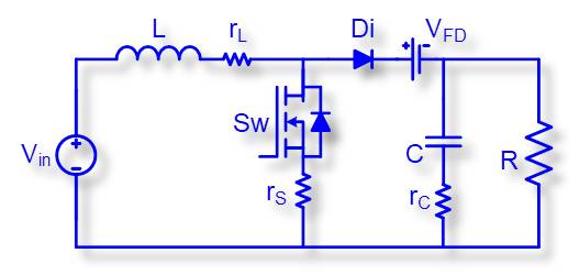
Fig. 3. Circuit configuration of conventional boost converter with non-idealities.
Voltage across inductor L:
Mode – I :

Mode – II :

Applying volt-sec balance on inductor (eqn. 5 and 6)

On solving eqn. 7
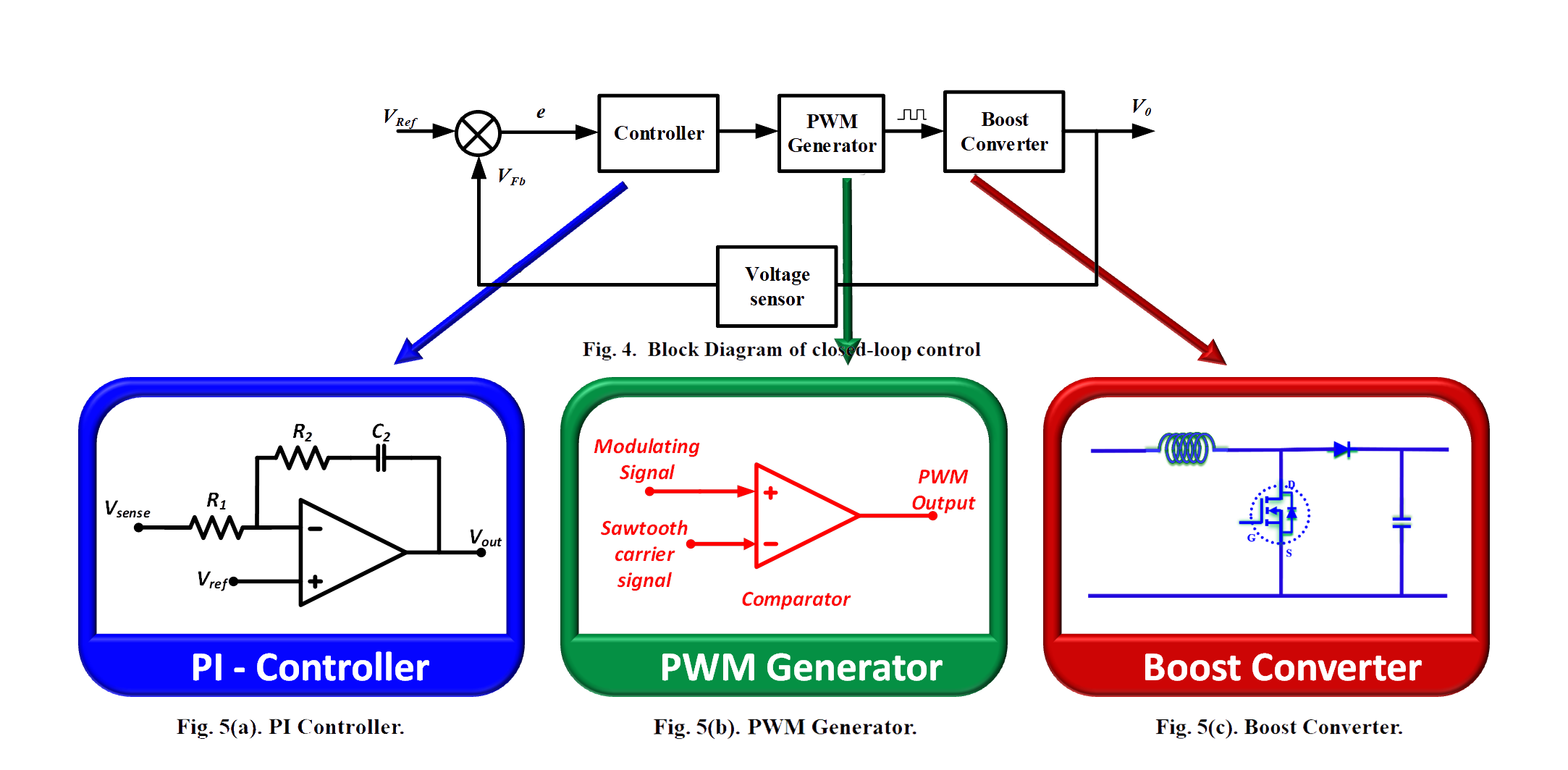
c) Voltage Regulation and Closed-loop Control:
In the event of battery voltage/load fluctuations, load voltage varies. However, DC-loads require constant voltage for their feasible/efficient operation, which demands automatic control. A simple PI-controller (proportional plus integral controller [2], see Fig. 5(a)) is capable of maintaining a constant load voltage despite the fluctuations (battery voltage/load). Here, the controller adjusts the pulse width of the PWM signal [2] according to the input error signal. As shown in Fig. 5(b), the error signal is the difference between the reference voltage and actual load voltage.