
Single phase IGBT inverter under sinusoidal PWM control
Theory
The circuit configuration of single-phase bridge inverter is shown in Fig. 1.
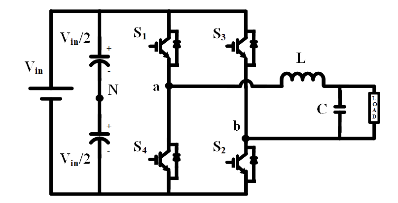
Fig. 1. Circuit diagram of single -phase bridge inverter.
Based on the operation of switches (S1, S2, S3, S4: ON/OFF-state) the operating principle of the inverter is explained below briefly. All possible switching states are given Table.1.
|
Switch (S1, S2): ON-state Switch (S3, S4): OFF-state |
Switch (S1, S2): OFF-state Switch (S3, S4): ON-state |
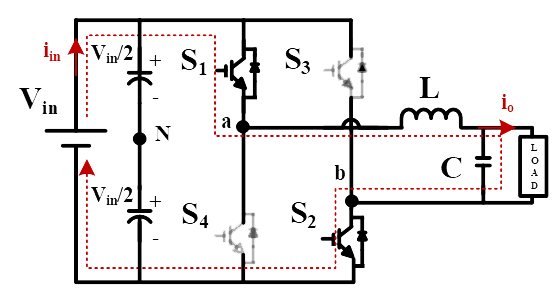
Fig. 2(a). Equivalent circuit when S1 and S2 are ON |
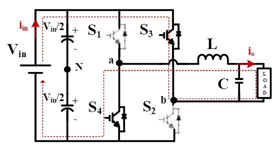
Fig. 2(b). when S3 and S4 are ON |
Table-1. Switch states for full bridge Inverter-Unipolar switching
| Switching States | S1 | S2 | S3 | S4 | Vo |
| 1 | ON | ON | OFF | OFF | Vin |
| 2 | OFF | OFF | ON | ON | -Vin |
| 3 | ON | OFF | ON | OFF | 0 |
| 4 | OFF | ON | OFF | ON | 0 |
MULTIPLE-PULSE WIDTH MODULATION
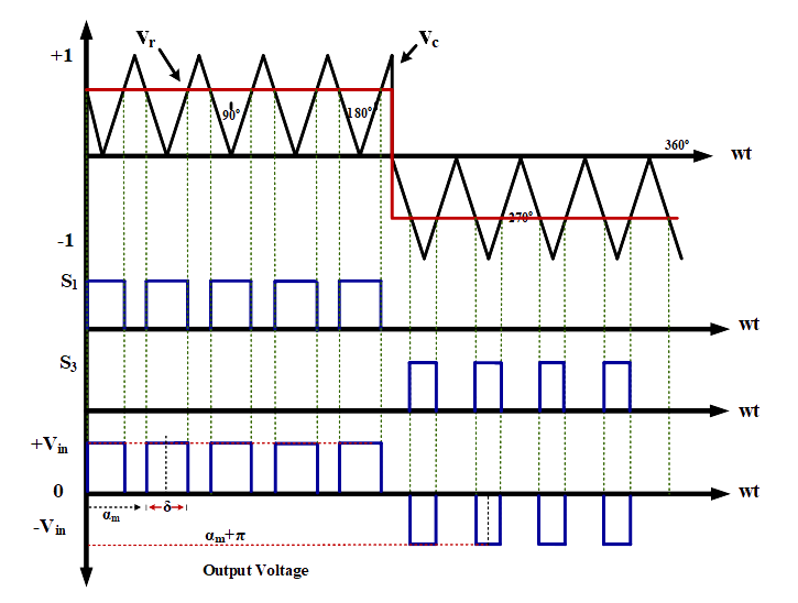
Fig. 3. Multi-pulse PWM generation.
- The harmonic content can easily be reduced by using several pulses in each half-cycle of output voltage.
- The generation of gating signals for turning ON and OFF of switches is done by comparing a square wave reference signal with triangular carrier wave.
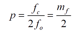
- The frequency of reference signals sets the output frequency (fo) and the carrier frequency (fc) determines the number of pulses (p) per half-cycle.
- The modulation index (M) controls the output voltage magnitude.
- This type of modulation is also known as uniform pulse-width modulation (UPWM).
- The number of pulses (p) per half-cycle is:
..(1)
where “mf=fc/fo” is defined as the frequency modulation ratio.
..(2)
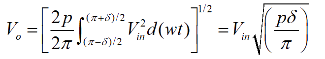
- The variation of the modulation index (M) from 0 to 1 varies the pulse width “d” from 0 to “T/2p” (0 to ℼ/p) and the RMS output voltage (Vo) from “0 to Vin”.
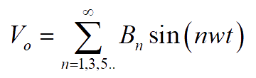
- The general form of load voltage expressed using Fourier series is
..(3)
The coefficient ‘Bn’ can be found by adding the effects of all pulses (2p).
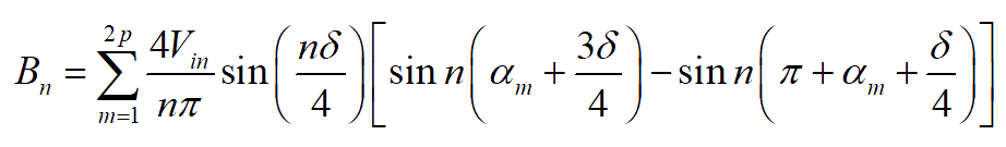
..(4)
- The pulse width ‘d’ is
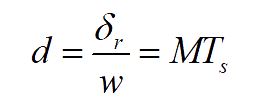
..(5)
where Ts=T/2p.
SINUSOIDAL-PULSE WIDTH MODULATION (SPWM)
- For realizing SPWM, a high-frequency triangular carrier wave is compared with a sinusoidal reference of the desired output frequency. (Unipolar PWM)
- The intersection of carrier and reference waveforms determines the switching instants of the devices.
- The PWM scheme is illustrated in Fig. 4 in which ‘vc’ is the peak value of triangular carrier wave and ‘vr’ that of the reference signal.
- The switches of the inverter are controlled based on the PWM generated above.
- When the instantaneous sinusoidal reference magnitude is higher than the triangular carrier magnitude then the PWM signal is high, otherwise it is low.
The calculation of the sinusoidal PWM output voltage is similar as that of the uniform PWM output voltage. However, for sinusoidal PWM, the width of each pulse varies according to its position. [1]
Fourier series expression for the output voltage waveform is:

..(6)
Since the inverter output voltage is an odd function, only odd harmonics exist. The calculation of the output voltage harmonic components can be done using a single pair pf pulses.

..(7)

..(8)
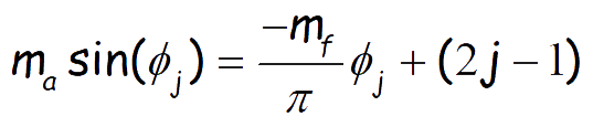
After solving, adding the contribution from all the other pulses, the ith component of vo is given by

..(9)
Approximating the pulse width
Assume each pulse is located at the discrete value of ϕi, which represents the first intersection for the generation of the ith pulse. Then the approximated mathematical relation for the width is found using a geometrical relation

..(10)
The approximated width of the ith pulse, is given by,
is given by,

..(11)
Since α = β, then

..(12)
Substituting the values will result in,

..(13)
The general expression for vcont(wt),

..(14)
The expression for the reference signal is given by

..(15)

..(16)
Equation can be rewritten as
..(17)
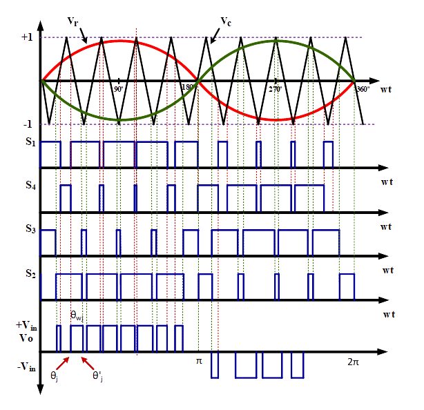
Fig. 4. Ideal waveforms for the unipolar SPWM generation.