Performance measurement and analysis of isolated DC-DC push-pull regulator
Theory
The circuit diagram of push-pull converter is given in Fig. 1.
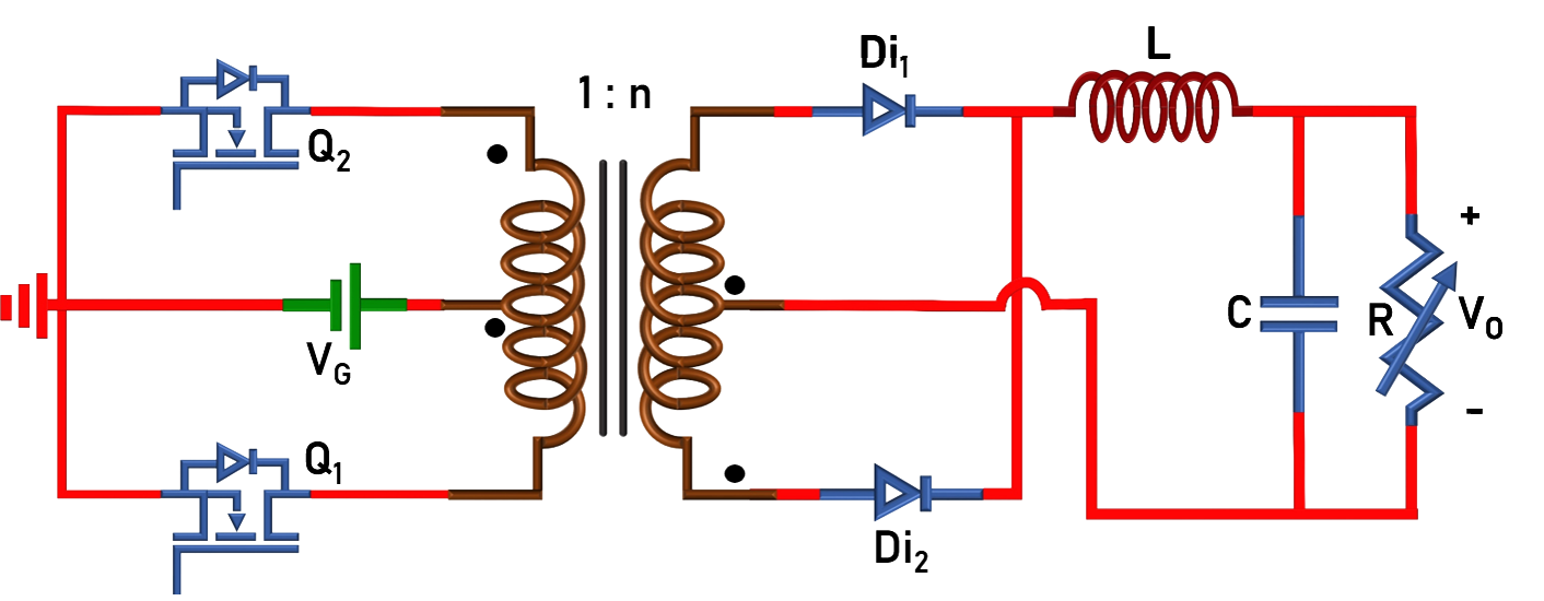
Fig. 1. Circuit Diagram of Push-pull Converter.
The switches (Q1 and Q2: ON/OFF-state) are turned-ON/OFF using 180° phase shifted PWM signals. The converter operation can easily be understood from the following equivalent circuits. Brief mathematical analysis is given below.
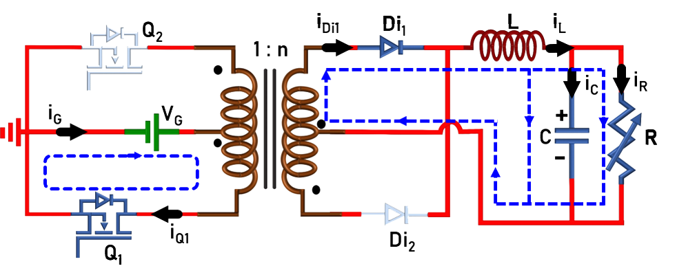
Fig. 2(a). Circuit in mode-I (Q1- ON, Q2- OFF). |
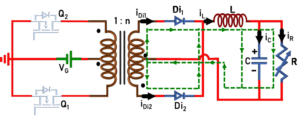
Fig. 2(b). Circuit in mode-II, IV (Q1- OFF, Q2- OFF). |
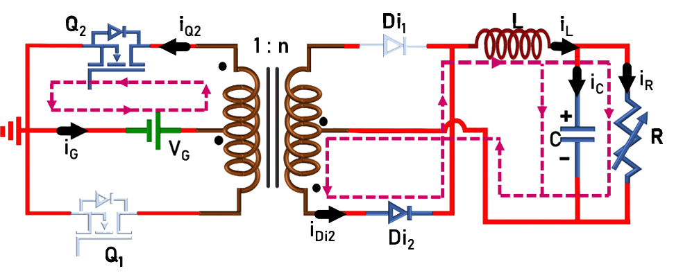
Fig. 2(c). Circuit in mode-III (Q1- OFF, Q2- ON). |
|
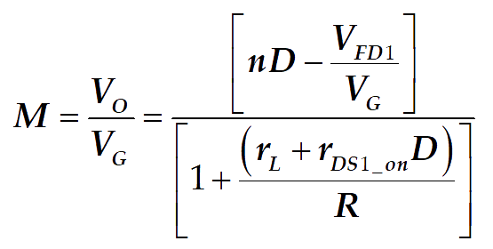
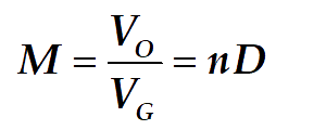
1. Voltage conversion ratio or voltage gain (M)
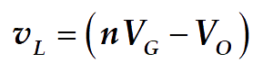
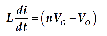
Voltage across inductor L:
Since the frequency of inductor current/voltage is ‘TS/2’, only Mode-I and Mode-II or Mode-III and Mode-IV is sufficient to formulate the voltage gain:
Mode – I :
where n=Ns/Np.
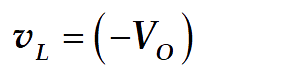
Mode – II :
Applying ‘volt-sec’ balance across the inductor (eqn. 1 and 2)
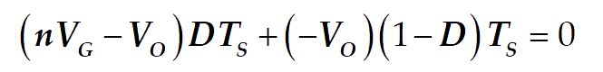
Solving eqn. 3 gives,
2. Average current through the inductor:
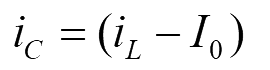
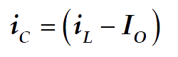
Current through capacitor C:
Since the frequency of both the inductor and capacitor currents is ‘TS/2’, only Mode-I and Mode-II is considered.
Mode – I :
Mode – II :
Applying ‘Charge-sec’ balance to the capacitor (eqn. 5 and 6)
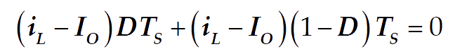
Solving eqn. 7 gives,
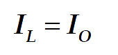
Therefore, average inductor current is equal to load current.
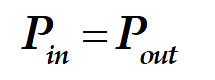
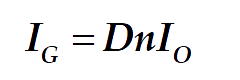
3. Power balance under ideal condition (neglecting losses in the converter):
In ideal conditions, the input power is equal to the output power. Hence,
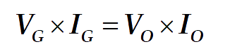
Substituting eqn. 4 in 10,
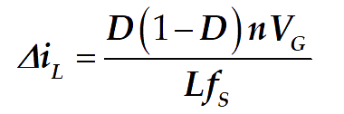
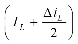
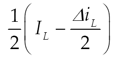
4. Inductor current ripple:
From eqn. 1,
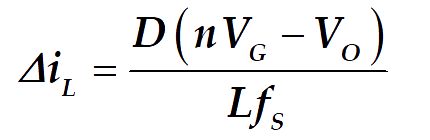
Therefore, the inductor ripple current is,
5. Current through various components:
The current through various components can easily be identified from Fig. 3.
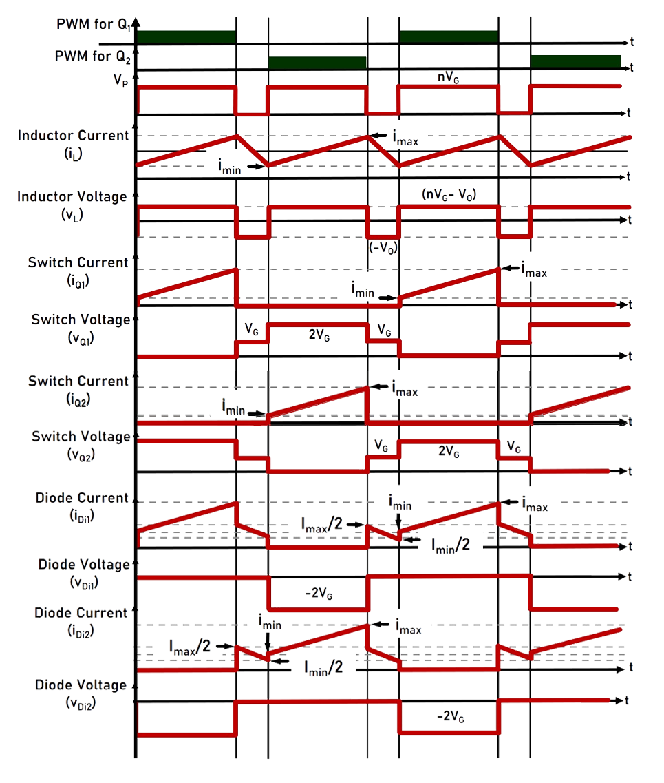
Fig. 3. Circuit Diagram of Push-pull Converter.
|
Mode-I (DTs/2) |
Mode-II (1-D)Ts |
Mode-III (DTs/2) |
Average Current | ||||
| imin | imax | imin | imax | imin | imax | Iavg | |
| iL | 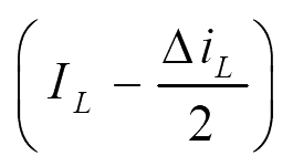 |
 |
|
|
|
|
 |
| iC |  |
 |
|
|
|
|
0 |
| iQ1 | 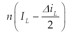 |
 |
0 | 0 | 0 | 0 |  |
| iQ2 | 0 | 0 | 0 | 0 |  |
 |
 |
| iDi1 |  |
 |
 |
 |
0 | 0 | 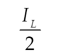 |
| iDi2 | 0 | 0 | 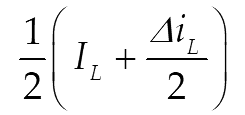 |
 |
 |
 |
 |
6. Voltage and current stress on various components:
| Voltage stress | Current Stress | |
| Inductor (L) | 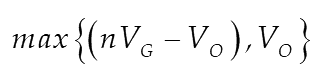 |
 |
| Capacitor (C) |  |
 |
| Switches (Q1, Q2) |  |
 |
| Diodes (Di1, Di2) |  |
 |
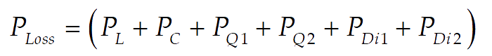
7. Efficiency analysis:
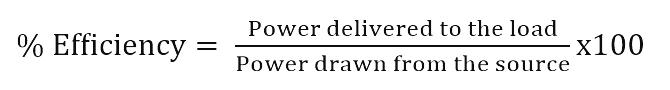
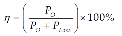
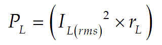
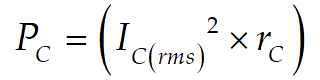
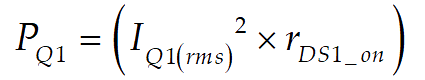
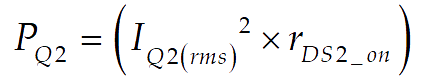
Power losses occurring in various components are given below:
Power loss in inductor:
Power loss in capacitor:
Power loss in switches:
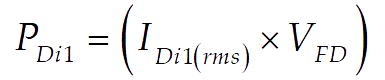
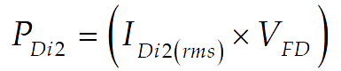
Power loss in diodes:
Total power loss:
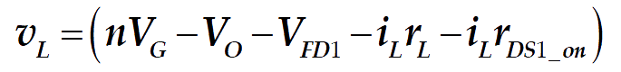
8. Effect of non-idealities on voltage gain expression:
Power losses occurring in various components are given below:
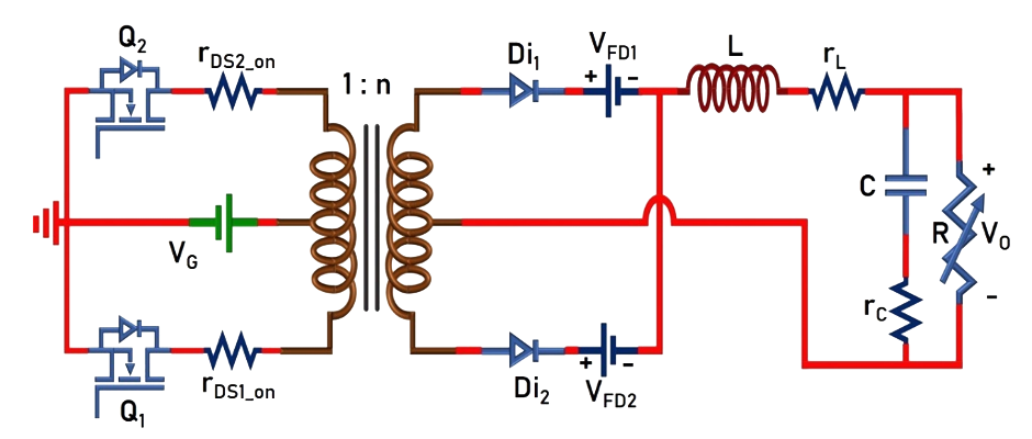
Fig. 4. Circuit Diagram of Push-pull Converter with non-idealities.
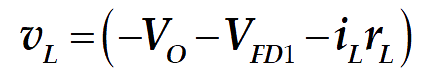
Voltage across inductor L
Since the frequency of inductor voltage is TS/2, only Mode-I and Mode-II or Mode-III and Mode-IV will be taken:
Mode – I :
Mode – II :
Applying Volt-sec balance across the inductor (eqn. 24 and 25),

Substituting,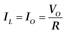 and solving the above equation gives,