
Verification of Maximum Power Transfer Theorem 
Procedure
Circuit Diagram
.jpg)
[Fig 1: Circuit diagram of experimental set-up for verification of maximum power transfer theorem]
1. When only XL is adjustable:
- Take a suitable set of values of Vs, XS, XL as shown in the figure. You can choose XS to be inductive (Ls) and capacitive (Cs). XL can choose as inductive(LL) and capacitive (CL) to the load.
- Next choose a suitable load resistance (RL).
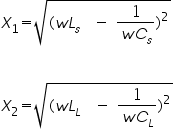
- For the maximum power theorem, the condition would be RL=RS, XS(i.e. X1)=-XL.(i.e. X2)
Where,

Take an example, put Ls=1mH, Cs=10.1µF.
Now for different value of Cs, note down V1 and V4.
Load power (PL) = I2*RL = I*I*RL = (V1/100)*V4
= K*V1*V4
where K=1/100 = 1/Rs
Enter the value of the voltage for different values of Cs and obtain the set corresponding to the maximum value of (V1*V4). Verify that for this set V2=V6.
2. When only RL is adjustable:
Repeat the procedure of part (1), with Cs fixed and RL varied. At the point of maximum power check $$R_L=\sqrt(R_s^2 + (X_1 + X_2)^2)$$ and VRL=V4.
3. When both RL and XL are adjustable:
Repeat the procedure of part (2), varying Cs and obtain the maximum power condition.
Check under this condition,
VRL= VRS i.e. V1=V4 ;
VLS= VCL i.e. V2=V6 ;