
Extraction of diode SPICE parameters related to Capacitance-Voltage (C-V) 
Theory
Introduction:
Extraction of Diode SPICE C-V Parameters
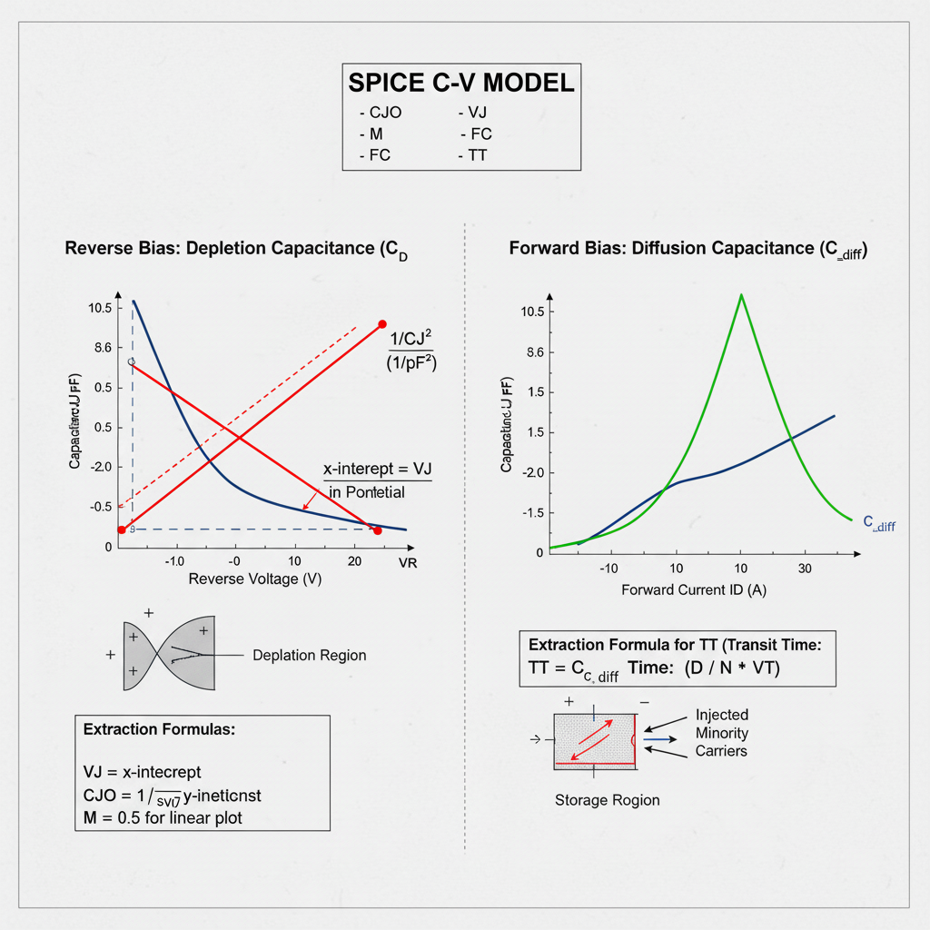
Fig. 1. Graphical Extraction of Diode SPICE I-V Parameters
The capacitance of a p-n junction is not constant; it varies with the applied voltage. The total capacitance ($C_J$) modeled in SPICE is the sum of two distinct physical components:
- Depletion Capacitance ($C_D$ or $C_j$): Dominant under reverse bias.
- Diffusion Capacitance ($C_{diff}$): Dominant under forward bias.
$$C_J = C_D + C_{diff}$$
The extraction process involves separating these two components and finding the SPICE parameters that govern their behavior.
1. Depletion Capacitance ($C_D$)
This capacitance arises from the charge stored in the depletion region (or space-charge region) at the p-n junction. As the reverse voltage increases, the depletion region widens, changing the amount of stored charge.
Key SPICE Parameters
CJO(Zero-Bias Junction Capacitance): The value of the depletion capacitance when the applied voltage $V_D$ is zero.VJ(Junction Potential): Also known asPB, this is the built-in potential (e.g., ~0.6-0.8V for silicon) of the junction.M(Grading Coefficient): Describes the doping profile of the junction.M = 0.5for an abrupt (step) junction.M = 0.33for a linearly graded junction.
FC(Forward-Bias Capacitance Coefficient): A fitting parameter (default 0.5) used to linearize the capacitance equation under forward bias to prevent the model from becoming singular at $V_D = VJ$.
The Model Equation
The standard SPICE equation for depletion capacitance under reverse bias ($V_D < FC \cdot VJ$) is:
$$C_D = \frac{CJO}{(1 - V_D / VJ)^M}$$
(Note: For reverse bias, $V_D$ is negative, so the denominator increases as reverse bias increases, and capacitance decreases.)
Extraction Method: The $1/C^2$ Plot
The parameters CJO, VJ, and M are extracted from C-V measurements taken under reverse bias, where $C_J \approx C_D$.
The extraction method linearizes the model equation. For the most common case of an abrupt junction (M = 0.5), we can square and invert the equation:
$$C_D^2 = \frac{CJO^2}{(1 - V_D / VJ)}$$
$$\frac{1}{C_D^2} = \frac{1 - V_D / VJ}{CJO^2} = \left( \frac{1}{CJO^2} \right) - \left( \frac{1}{CJO^2 \cdot VJ} \right) \cdot V_D$$
This equation is in the linear form $y = b + m \cdot x$, where:
- $y = 1/C_D^2$
- $x = V_D$ (the applied voltage)
- $b = 1/CJO^2$ (the y-intercept)
- $m = -1 / (CJO^2 \cdot VJ)$ (the slope)
Extraction Procedure:
- Measure C-V: Measure the diode's capacitance $C_J$ at several reverse bias voltages $V_D$ (e.g., from 0V to -10V).
- Plot Data: Create a plot of $1/C_J^2$ (y-axis) versus $V_D$ (x-axis). The data should form a straight line.
- Extract
VJ: Extend the straight line to the x-axis (where $y=0$). The x-intercept is the junction potential,VJ. - Extract
CJO: The y-intercept (at $V_D = 0$) is $1/CJO^2$. Therefore,CJOis calculated as: $$CJO = \frac{1}{\sqrt{\text{y-intercept}}}$$ - Verify
M: If the plot is indeed a straight line, the assumption thatM = 0.5is correct. If the plot is curved, a different value ofMmay be needed (e.g., plot $1/C_J^3$ forM=0.33).
2. Diffusion Capacitance ($C_{diff}$)
This capacitance arises from the charge of minority carriers injected into the quasi-neutral regions during forward bias. It is directly related to the forward current $I_D$ and the time it takes for these carriers to recombine.
Key SPICE Parameter
TT(Transit Time): Represents the mean time for injected minority carriers to transit through the neutral region (or recombine).
The Model Equation
The diffusion capacitance is defined as the change in stored minority charge ($Q_{diff}$) with respect to the junction voltage ($V_j$):
$$C_{diff} = \frac{dQ_{diff}}{dV_j}$$
The stored charge is $Q_{diff} = I_D \cdot TT$. The dynamic conductance of the diode is $g_d = dI_D/dV_j$. This leads to the model equation:
$$C_{diff} = TT \cdot \frac{dI_D}{dV_j} \approx TT \cdot \frac{I_D}{N \cdot V_T}$$
Where $N$ is the ideality factor and $V_T$ is the thermal voltage (both extracted from I-V measurements).
Extraction Method
The transit time TT must be extracted from measurements taken under forward bias, where $C_J = C_D + C_{diff}$.
Extraction Procedure:
- Measure C-V in Forward Bias: Measure the total capacitance $C_J$ at a specific forward current $I_D$ (and its corresponding voltage $V_D$).
- Calculate $C_D$: At this $V_D$, the depletion capacitance $C_D$ is still present. It is calculated using the forward-bias part of its model (which uses the
FCparameter). - Isolate $C_{diff}$: Subtract the calculated depletion capacitance from the total measured capacitance: $$C_{diff} = C_{J, \text{measured}} - C_{D, \text{calculated}}$$
- Extract
TT: Re-arrange the model equation to solve forTT. You will need the values of $I_D$, $N$, and $V_T$ (from I-V analysis) at the bias point. $$TT = \frac{C_{diff}}{g_d} = \frac{C_{diff}}{(I_D / (N \cdot V_T))}$$
This gives the value for TT, completing the C-V parameter extraction.