
Extraction of bipolar SPICE Gummel-Poon parameters related to forward Output (Ic vs. Vc) characteristics 
Theory
Introduction:
BJT Parameter Extraction from Forward Output Characteristics
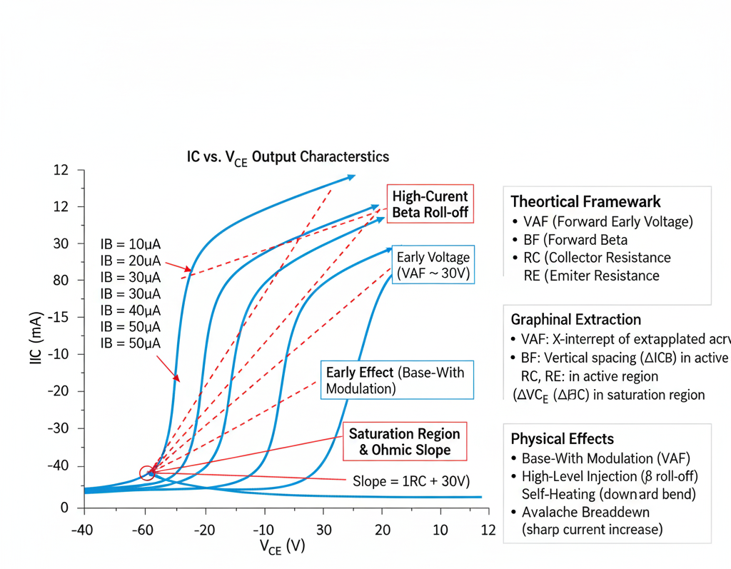
Fig. 1. Forward I-V Characteristic & Parameter Extraction
Introduction
The forward output characteristic plot is a fundamental measurement for Bipolar Junction Transistors (BJTs). It provides crucial information about the transistor's behavior in the forward-active and saturation regions.
This plot is generated by applying a constant, stepped Base Current ($I_B$) and sweeping the Collector-Emitter Voltage ($V_{CE}$), while measuring the resulting Collector Current ($I_C$).
This plot ($I_C$ vs. $V_{CE}$) is used to extract key SPICE parameters that model the transistor's output conductance, saturation, and parasitic resistances.
Key SPICE Parameters
The primary parameters extracted from this plot are:
VAF(Forward Early Voltage): Models the slope of the $I_C$ curve in the forward-active region.RC(Collector Series Resistance): Models the parasitic resistance in the collector.RE(Emitter Series Resistance): Models the parasitic resistance in the emitter.
While the Forward Beta (BF) is visualized on this plot (as the spacing between curves), its ideal value is more accurately extracted from the Gummel plot.
1. Forward-Active Region: The Early Effect
In the ideal forward-active region, the collector current ($I_C$) should be independent of the collector-emitter voltage ($V_{CE}$). However, in a real BJT, $I_C$ gradually increases with $V_{CE}$.
Physical Cause: This phenomenon is called base-width modulation, or the Early effect. As $V_{CE}$ increases, the reverse bias across the collector-base junction increases. This widens the collector-base depletion region, which encroaches into the neutral base, reducing the effective base width. A narrower base increases the gradient of the minority carrier concentration, thus increasing the collector current.
SPICE Model: This effect is modeled by the Forward Early Voltage (
VAF). The collector current is modified by a factor:$$I_C = I_{C,ideal} \cdot \left( 1 + \frac{V_{CE}}{VAF} \right)$$
Extraction Method:
- On the $I_C$ vs. $V_{CE}$ plot, draw a tangent line along the linear, sloped portion of each curve in the active region.
- Extrapolate these lines backward until they intersect the horizontal ($V_{CE}$) axis.
- Ideally, all lines will converge at a single point on the negative $V_{CE}$ axis. The absolute value of this voltage intercept is the Forward Early Voltage (
VAF).
A very large
VAF(a far-left intercept) corresponds to very flat curves, indicating a near-ideal current source. A smallVAFcorresponds to steeply sloped curves.
2. Saturation Region: Parasitic Resistances
The saturation region is the area of the plot at low $V_{CE}$ (the "knee") where $I_C$ rises sharply before flattening out. In this region, the transistor acts less like a current source and more like a simple "on-resistance" ($R_{on}$).
Physical Cause: This "on-resistance" is dominated by the parasitic series resistances in the collector and emitter, modeled by
RCandRE.SPICE Model: The total collector-emitter saturation voltage ($V_{CE,sat}$) is the sum of the internal junction voltages and the voltage drops across these parasitic resistors:
$$V_{CE,sat} \approx V_{CE,sat,internal} + I_C \cdot RC + I_E \cdot RE$$
Since $I_E \approx I_C$ at high gain, this simplifies to:
$$V_{CE,sat} \approx V_{CE,sat,internal} + I_C \cdot (RC + RE)$$
Extraction Method:
- The parameters
RCandREare extracted from the slope of the $I_C$ vs. $V_{CE}$ curves in the deep saturation region. This slope represents the "on-resistance": $$R_{on} = \frac{\Delta V_{CE}}{\Delta I_C} \approx RC + RE$$ - Specialized methods (e.g., the "open-collector" method or comparing slopes at different $I_B$ levels) are required to separate the individual contributions of
RCandREfrom the total measured resistance. - A large
RCalso causes the "knee" to be "softer," an effect known as quasi-saturation. This is because the internal $I_C \cdot RC$ voltage drop causes the internal base-collector junction to become forward-biased before the external $V_{CE}$ drops to its saturation level.
- The parameters
Other Observable Effects
- High-Current Beta Roll-Off: At high collector currents, the curves will appear to "bunch up" or "crowd together." This means the vertical spacing (which represents $\Delta I_C$) for a constant $\Delta I_B$ decreases, visualizing the drop in current gain (beta).
- Self-Heating: At high power levels (both high $I_C$ and high $V_{CE}$), the device heats up. This can cause the $I_C$ curves to bend downward as $V_{CE}$ increases, because gain typically decreases at higher temperatures.
- Breakdown: At very high $V_{CE}$ (beyond the normal operating range), the $I_C$ curves will suddenly and sharply turn upward. This is avalanche breakdown of the collector-base junction.