Shift registers 
Procedure
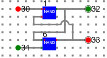
- Design Latch circuit and make a component say ‘Latch’.

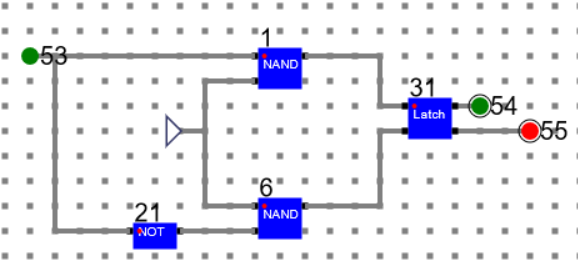
- Using the latch, design a D-FF and make a component as shown below.

Circuit Diagram of a SISO (Serial In/Serial Out) Shift Register
We have designed D-FF as shown in earlier experiment and used the same here to design a shift register. We have used 1 bit memory element to store the output bit from each D-FF in the circuit.
Step 1: (Initial State)

The input bit is 157.
The output bits are 159, 160, 161, 162.
Initially register contains no data.
Step 2:

Input Bit: 157:1 and clock.
Output Bit: 159: 1
Step 3:

Input Bit: 157:1 and clock.
Output Bit: 159: 1, 160:1
Step 4:

Input Bit: 157:0 and clock.
Output Bit: 159: 0, 160:1, 161:1
Step 5:

Input Bit: 157:1 and clock.
Output Bit: 159: 1, 160:0, 161:1, 162:1
Step 6:

Input Bit: 157:0 and clock.
Output Bit: 159: 0, 160:1, 161:0, 162:1
At each clock pulse, all bits are shifted one step to the right and stored in the register.
Manual
Follow the below manual and perform the experiment
- Manual --> Click Here
