
Metal-Semiconductor Junctions
Metal-semiconductor junctions form the backbone of modern electronic and optoelectronic devices. These junctions control current flow and charge carrier dynamics, making them fundamental in semiconductor physics and engineering. Understanding their operation, characteristics, and applications is essential for designing efficient electronic components.
Semiconductor Basics
Semiconductors are materials whose electrical properties lie between conductors and insulators. Their conductivity can be significantly modified by introducing impurities, a process known as doping.
- n-type Semiconductors: Created by doping with elements that have more valence electrons than the semiconductor (e.g., phosphorus in silicon). This introduces extra electrons, increasing the negative charge carrier density.
- p-type Semiconductors: Achieved by doping with elements that have fewer valence electrons (e.g., boron in silicon). This creates holes—positively charged mobile carriers.
Doping is essential for forming junctions, which lead to various electronic functionalities by modifying charge carrier distributions. Work function is defined as the amount of work required to remove electrons from the solid material (Fermi level) to free space vacuum. Electron affinity for a semiconductor is the work required to remove an electron from Ec (conduction band) to free space.
Metal-Semiconductor Junctions
When a metal comes into contact with a semiconductor, different types of junctions can form based on their electrical behavior and energy band alignment.
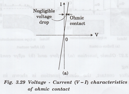
Ohmic Contacts
- Definition: Ohmic contacts provide a low-resistance electrical connection, allowing current to flow easily in both directions without significant rectification. The current-voltage (I-V) characteristics are linear and symmetric about the origin. he current is directly proportional to the potential across the junction and it is symmetric about the origin.Thus, ohmic contacts are non-rectifying and show negligible voltage drop and resistance irrespective of the direction and magnitude of current. When the n-type semiconductor has a higher work function than that of metal, or p-type has lower work function than that of the metal , then the junction formed is called the Ohmic junction.
- Formation: Achieving an ohmic contact typically requires heavy doping near the interface to ensure sufficient charge carriers are available for conduction. Techniques such as thermal annealing can improve the contact quality by reducing defects and enhancing carrier mobility.
- Metal selection is crucial—metals with a work function close to the semiconductor's electron affinity help minimize contact resistance.
- Good Ohmic Contact: When ρ (resistivity) is very small (high doping, clean interface), even a small voltage difference can result in a large current density.
- Poor Ohmic Contact: If ρ is large (due to poor interface quality, low doping, or barrier formation), the current density will be small, indicating more resistance at the interface.
- Example: An ohmic contact can be formed between heavily doped n-type silicon and metals like aluminum. The high doping level provides an abundance of free electrons, while aluminum facilitates easy electron flow, resulting in a junction that behaves like a simple resistor.
Schottky Barriers
Definition: A Schottky barrier is formed when a metal with a higher work function contacts a n-type semiconductor, or metal with lower work function contacts with p-type semiconductor with higer work function creating a rectifying junction. This results in a potential energy barrier that controls carrier injection and flow. Formation- height of schottky barrier is determined by the difference between the metal work function and the semiconductor electron affinity :

- For n-type semiconductors, a large Schottky barrier restricts electron flow from the metal into the semiconductor, leading to rectifying behavior.
- For p-type semiconductors, a similar effect occurs, but with holes as the majority carriers.
Applications: Schottky barriers are widely used in Schottky diodes, which have fast switching speeds and are employed in high-frequency applications.
Introduction to Semiconductor Heterojunctions
A heterojunction is formed at the interface between two different semiconductor materials with distinct band gaps and electron affinities.
Band Alignment in Heterojunctions
There are three types of band alignment in semiconductor heterojunctions:
- Straddling Gap (Type I): The conduction band minimum and valence band maximum of one semiconductor lie within the band gap of the other. This structure is commonly used in optoelectronic devices like LEDs and lasers.
- Staggered Gap (Type II): The conduction and valence bands of both semiconductors are offset, leading to spatial separation of charge carriers—useful in photodetectors.
- Broken Gap (Type III): The conduction band of one semiconductor is lower than the valence band of the other, leading to unique carrier transport properties useful in tunnel devices.
Applications of Heterojunctions
- High-Efficiency Solar Cells: Heterojunctions improve carrier separation and minimize recombination losses, enhancing photovoltaic efficiency.
- Light-Emitting Diodes (LEDs) and Lasers: Straddling gap heterojunctions enable efficient radiative recombination of electrons and holes.
- High-Electron Mobility Transistors (HEMTs): These transistors exploit the discontinuity in conduction bands to achieve high-speed operation.
Summary
- Metal-semiconductor junctions can be either ohmic contacts (low-resistance) or Schottky barriers (rectifying behavior).
- Contact resistance and doping levels play crucial roles in determining the electrical characteristics of metal-semiconductor interfaces.
- Semiconductor heterojunctions allow for engineered band alignments, enabling advanced applications in optoelectronics and high-speed transistors.
They are fast switching devices with low forward voltage drop. Used in power rectifiers, RF detectors, and clamping circuits.