
Kronig-Penney Model and Formation of Energy Bands
1. Getting Started
- Open the simulation page.
- You will see the Control Panel on the left, the Visualization Canvas in the center, and the Info Panel on the right.
- By default, the "Explore" mode is active.
2. Exploring Material Presets
- Go to the Material Presets section in the left panel.
- Click on Conductor: Observe how the energy bands are wide and may overlap. The band gap is virtually non-existent.
- Click on Semiconductor: Notice the appearance of distinct band gaps between the allowed energy bands.
- Click on Insulator: Observe the very wide band gaps that form, preventing electron flow.
3. Custom Experimentation
- Select the Custom preset.
- Vary Potential Depth (V0): Use the slider to increase V0. Watch how the band gaps widen as the potential barrier increases.
- Vary Well Width (a): Adjust the well width and observe changes in the wave functions and energy levels.
- Vary Barrier Width (b): Adjust the barrier width slider. A wider barrier increases the effective confinement, which significantly widens the band gap even at the same V0 and a.
4. Guided Learning
- Click on the Guided tab in the "Learning Mode" section.
- Follow the on-screen prompts (toasts) and step indicators to systematically explore the model.
5. Visualization Options
- Use the Display Options checkboxes to toggle:
- Potential Wells (Green lines)
- Energy Bands (Blue lines)
- Wave Functions (Red curves)
- Band Gaps (Red shaded regions)
- Switch views using the buttons above the canvas:
- Combined: Shows everything.
- Potential: Focuses on the lattice structure.
- E-k Diagram: Shows the dispersion relation.
Simulation Screenshots
Below are the screenshots from the Kronig-Penney model simulation:
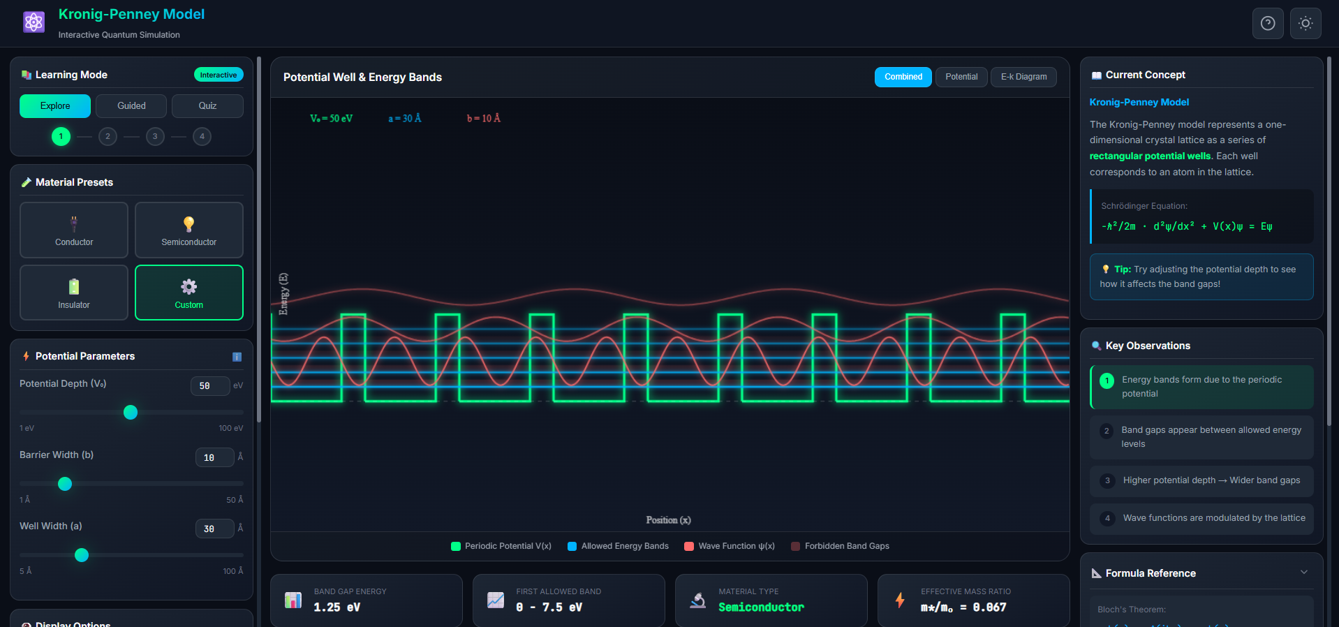 Figure 1: Main simulation interface showing the control panel, visualization canvas, and info panel.
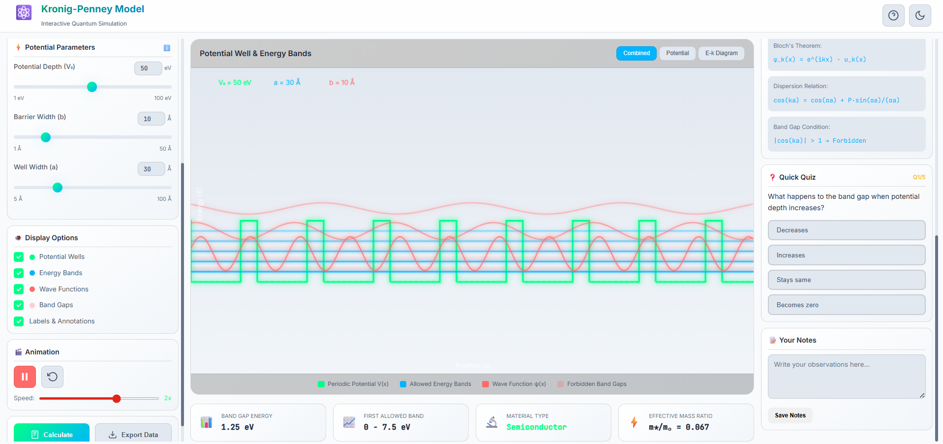 Figure 2: Energy band structure and wave functions for different material types.
Observation Table
Record your observations for different potential depths, well widths, and barrier widths below:
| S.No. | Potential Depth (V0) (eV) | Well Width (a) (Å) | Barrier Width (b) (Å) | Observed Band Gap (eV) | Material Type |
|---|---|---|---|---|---|
| 1 | 5 | 30 | 10 | ~0.13 | Conductor |
| 2 | 15 | 30 | 30 | ~0.75 | Semiconductor |
| 3 | 80 | 30 | 30 | ~4.00 | Insulator |
| 4 | 50 | 20 | 35 | ~3.18 | Insulator |
| 5 | 20 | 40 | 20 | ~0.67 | Semiconductor |
6. Quiz and Analysis
- Switch to Quiz mode to test your understanding.
- Use the Calculate button to verify the band gap values.
- Save your findings in the Notes section.