
Hartley Oscillator
Procedure
COMPONENTS
Transistors, Bread board, resistors, capacitors, inductance coil, dc power supply, C.R.O, connection wires etc
1. DESIGNING
Selection of transistor: Use high-frequency transistor BF195, NPN transistor.
Component specification:
- IC (MAX): 30 mA
- VCEO (MAX): 20 V
- βMIN: 36
- βMAX: 125
Design of amplifier section
Design of
Design of
Design of and .
Selection of capacitors : All capacitor values may be taken 1μF
Design of feedback network: Required frequency of oscillation
Procedure for simulator
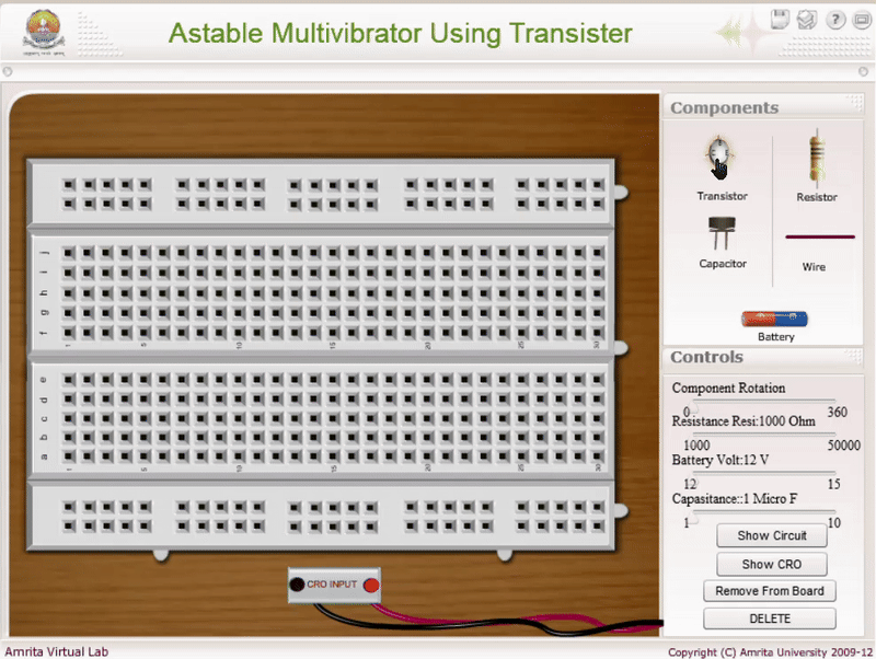
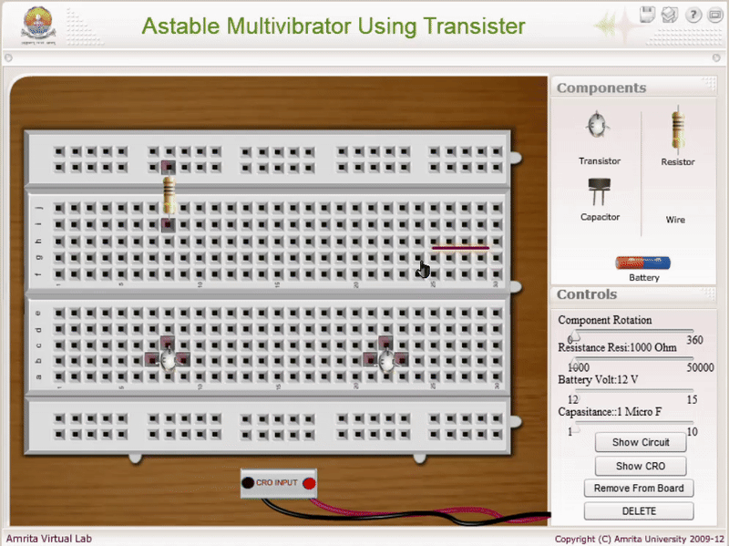
- Begin by arranging the components on the virtual breadboard as shown in Animation 1. Refer to the visual guide carefully to place each component in its correct position.
- To connect the components, click on one end of the wire and then click on the corresponding point on the breadboard to complete the connection. Repeat this step to interconnect all necessary components.
- Follow the connection diagram to ensure the circuit is completed correctly. Double-check that all connections are made as shown in the schematic.
- Once the circuit is fully connected, click the "Show CRO" button in the simulator interface. This will display the waveform output on the virtual Cathode Ray Oscilloscope (CRO).
To Change the Component Value
- Select the component whose value you want to modify by clicking on it within the simulator.
- Use the slider on the right-hand side of the simulator to adjust the value (e.g., resistance, capacitance) as needed for the experiment.
Result
Amplitude and frequency of sine wave from Hartley Oscillator = …… V, …… Hz.
WORKING
The connections are made as shown in fig.
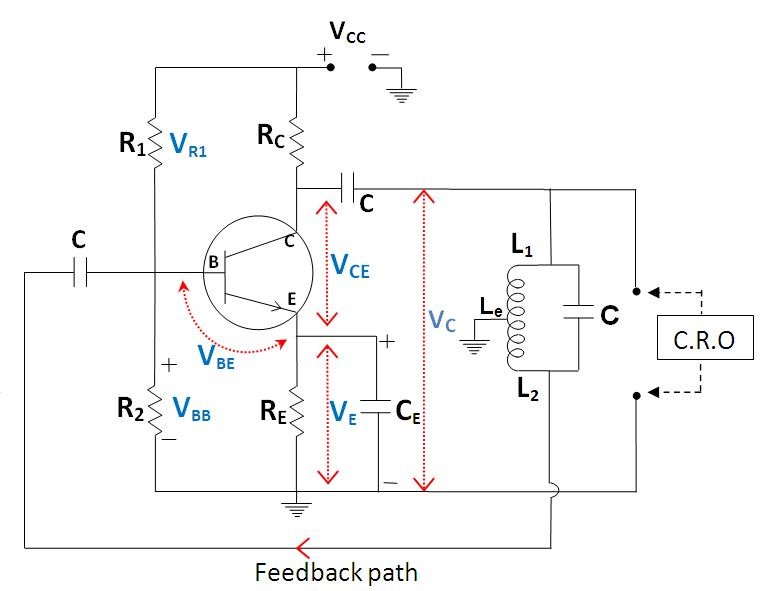
The collector of the transistor is connected to the positive terminal of the power supply (VCC) through the resistance RC. The resistances R1 and R2 are connected in series with the power supply. The resistance RE and the capacitor CE are connected in the emitter circuit. The negative terminal of the power supply and emitter resistance RE is earthed.
An inductance coil L connected in parallel with the capacitor C forms the tank circuit. The centre tap of coil L is earthed.
After making connections, the power supply is switched on. The frequency of oscillations is measured using a C.R.O.