
Generation of Clock Pulse using NAND gate.
Procedure
- Click on the Component button to place components on the table.


")
")
Fig. 1 Components
- Make connections as per the circuit diagram and pin diagram of IC or according to connection table.
- Connect the C.R.O on output terminal of circuit (Refer connection table).
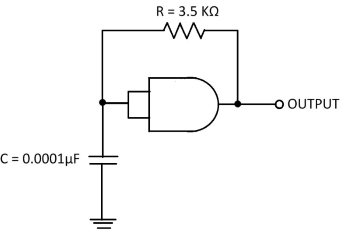
Fig. 2 Circuit diagram of clock pulse using NAND gate
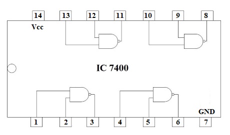
Fig. 3 Pin diagram of IC 7400
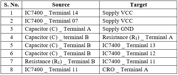
Table 1: Connection table
- Click on Check Connections button. If connections are right, click on ‘OK’, then Simulation will become active.
- Connect CH1/CH2 of C.R.O. to output terminal of the circuit.
- Observe output wave on C.R.O by adjusting C.R.O channel CH1/CH2 and TIME knobs.
- Use X Shift and Y Shift buttons for wave shifting.
- Measure the time period of output wave at C.R.O. and calculate the frequency by feeding the time period in the given box.
- Compare both experimental and theoretical frequencies.
- Click on the Reset button to reset the page.