Experiment name
MOS Capacitor: A Detailed Overview
Introduction
A MOS (Metal-Oxide-Semiconductor) capacitor is one of the fundamental building blocks in semiconductor devices and forms the basis of MOSFETs (Metal-Oxide-Semiconductor Field-Effect Transistors). It consists of a metal gate, an insulating oxide layer, and a semiconductor substrate. Understanding the MOS capacitor is critical to grasp modern electronic device operation.
Structure
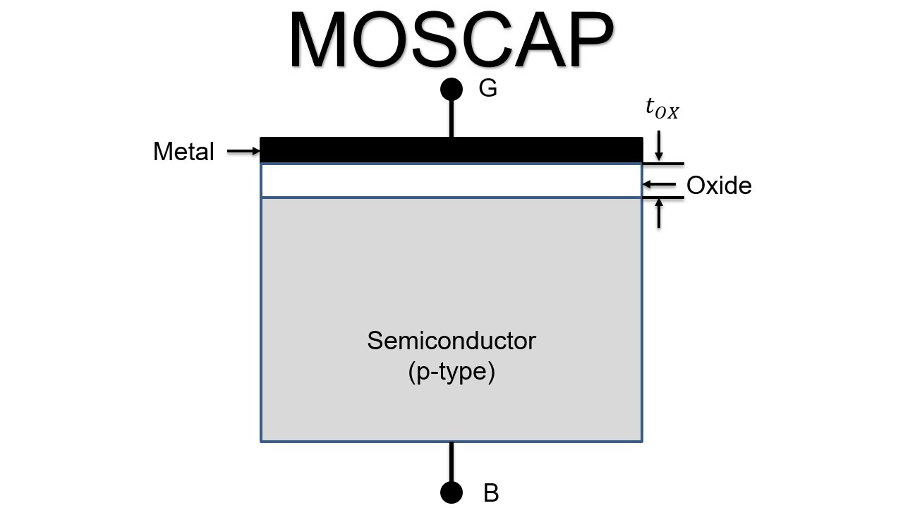
A typical MOS capacitor consists of three layers:
- Metal: Acts as the gate terminal (e.g., aluminum or polysilicon).
- Oxide Layer: An insulating layer, typically silicon dioxide (SiO₂), separating the metal and semiconductor.
- Semiconductor: A silicon substrate, which can be p-type or n-type depending on doping.
Diagram
Below is an example diagram of a MOS capacitor structure:

Working Principle
The MOS capacitor works by applying a voltage to the metal gate, which controls the charge distribution in the semiconductor. Depending on the voltage applied, three distinct modes occur:
1. Accumulation
- Condition: Negative voltage applied to the gate (for p-type substrate).
- Effect: Electrons are repelled from the gate, and holes accumulate at the oxide-semiconductor interface.
2. Depletion
- Condition: Small positive voltage applied to the gate.
- Effect: Holes are repelled from the interface, leaving behind negatively charged ions, forming a depletion region.
3. Inversion
- Condition: Higher positive voltage applied to the gate.
- Effect: The depletion region widens, and free electrons from the substrate are attracted to the interface, forming an inversion layer (n-type region in a p-type substrate).
Key Parameters
1. Threshold Voltage V_th
The voltage at which inversion begins. It depends on:
- Work function difference between the metal and semiconductor.
- Doping concentration in the substrate.
- Oxide thickness.
2. Capacitance C
- Accumulation and Inversion: Capacitance is constant and determined by the oxide layer.
- Depletion: Capacitance decreases as the depletion region width increases.
Energy Band Diagrams
1. Flat-Band Condition
- No net charge in the semiconductor.
- The energy bands are flat, with no bending.
2. Accumulation
- Energy bands bend upward.
- Holes accumulate at the interface.
3. Depletion
- Energy bands bend downward, away from the Fermi level.
- The region near the oxide interface becomes depleted of majority carriers.
4. Inversion
- Bands bend significantly downward.
- The minority carrier concentration exceeds that of the majority carriers near the interface.
Mathematical Analysis
Capacitance
The total capacitance can be expressed as:
1 / C_total = 1 / C_ox + 1 / C_depl
Where:
C_total: Total capacitance of the MOS capacitor.
C_ox: Capacitance due to the oxide layer.
C_depl: Capacitance due to the depletion region.
--
Applications
- MOSFETs: MOS capacitors form the gate structure in MOSFETs.
- Dynamic RAM: Used to store charge in memory cells.
- Sensors: MOS structures are used in gas sensors and other semiconductor-based sensors.
Summary
The MOS capacitor is a simple yet versatile device critical for modern electronics. It showcases how electric fields control charge distribution, forming the foundation for transistors and memory devices. Mastering its working is a stepping stone for understanding semiconductor physics and device engineering.
References
- "Semiconductor Device Fundamentals" by Robert F. Pierret.
- Online materials from IEEE Xplore and similar educational sources.
