
Combinational Logic Design 
Assignment Statements for Ripple Carry Adder:
- Create a half adder circuit using only logic gates and test it by giving proper input.
- Create a full adder circuit using only logic gates and test it by giving proper input.
- Create a full adder circuit using half adder and test it by giving proper input.
- Create a 4-bit ripple carry adder circuit using half adders and full adders and test it by giving proper input.
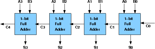
Circuit diagram of Ripple Carry Adder:
Procedure
- To draw any diagram in the simulator please follow the manual given in manual section.
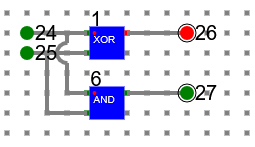
- Half Adder with ‘XOR’ and ‘AND’ gates readily available in the simulator.
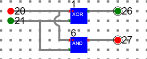
20, 21: Input bits
26: Sum
27: Carry
- This could be saved as a component with suitable name – say ‘HalfAdder’.
- Full Adder with ‘XOR’, ‘AND’ and ‘OR’ gates readily available in the simulator.
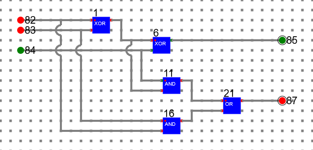
where
82, 83: Input Bits
84: Carry-In
85: Sum
87: Carry-Out
- Full Adder with the help of Half Adders (Designed Above) and ‘OR’ gate
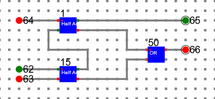
1, 15: Half Adders
62, 63: Input Bits
64: Carry-In
65: Sum
66: Carry Out
- This could be saved as a component with suitable name – say ‘FullAdder’.
- Ripple Carry Adder with 1 half adder and 3 full adders
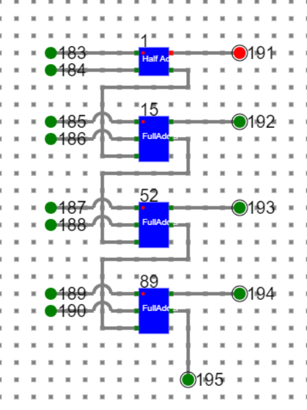
- 1: Half Adder and 15, 52, 89: Full Adder
- First 4 bit number represented by 183(LSB), 185, 187 and 189(MSB) and second 4 bit number represented by 184 (LSB), 186, 188, 190 (MSB).
- The output number after sum is 191 (LSB), 192, 193, 194 (MSB).
- Final carry-out is 195.
Assignment Statements for Carry-Lookahead Adder:
- Create a full adder circuit using basic logic gates and test it by giving proper input.
- Create a Pi-Gi generator circuit using basic logic gates and test it by giving proper input.
- Create 3 input AND gate, 3 input OR gate, 4 input AND gate, 4 input OR gates using basic logic gates and test it by giving proper input.
- Create a carry generator using above GATEs and test it with proper input
- Create a 4-bit carry lookahead adder circuit using Pi-Gi generator, carry generator and Full Adders.
Procedure
To draw any diagram in the simulator, please follow the instructions given in the manual.
- Create a Pi-Gi generator as shown below. For Pi-Gi, please refer to the theory section. Save this as a component, say pi-gi.
Pi-Gi generator
where
24: Ai, 25: Bi 26: Pi 27: Gi
- Create carry generator as shown in the picture below using basic AND gate, basic OR gate, 3 input AND, 3 input OR, 4 input AND, 4 input OR gates and save it as a component say c-gen.
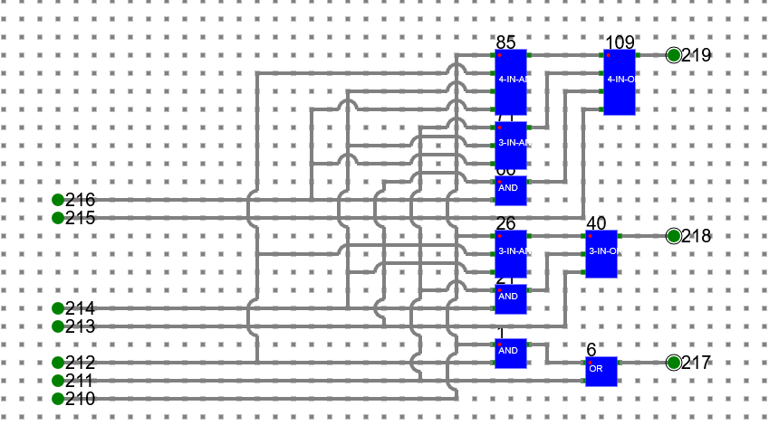
Carry Generator for 4 bit carry-lookahead adder
where
210: C1, 211: G1, 212: P1, 213: G2, 214: P2, 215: G3, 216: P3, 217: C2, 218: C3, 219: C4
- Create a 4 bit carry lookahead adder as shown below using Pi-Gi generator, c-gen and 1 bit Full Adder.
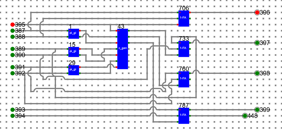
4-bit carry-lookahead adder
395: Cin, 387: A1, 388: B1, 389: A2, 390: B2, 391: A3, 392: B3, 393: A4, 394: B4, 396: S1, 397: S2, 398: S3, 399: S4
448: S5 [A1, B1: LSB A4, B4: MSB S1: LSB, S5: MSB]
Follow the below manual and perform the experiment
- Manual --> Click Here