Carrier Transport
In a semiconductor at room temperature, there are electrons and holes (there are more carriers in extrinsic semiconductor) moving around due to thermal energy. In a semiconductor devices, the device is designed to control the flow of carriers. The motion of the carriers is called transport. Here we will learn about the two transport mechanisms Drift and Diffusion which together make the electronic devices behave the way they behave.
Drift
Electrons in a semiconductor, move in the direction opposite to that of applied electric field E (force F= qE). Holes move in the direction of the applied electric field. As they are moving, they undergo collisions with vibrating Si atoms. This makes their movement unpredictable and random (similar to Brownian motion of gas particles). However, the net displacemnet of each charge carrier is along the electric field.The corresponding velocity (Drift velocity), which is the average velocity of the carrier, can be modeled as given below.
Note: Subscript n is used for electrons and p for holes in this experiment
Drift Velocity Formulas
for electrons:
for holes:
Where:
Mobility is the proportionality constant and depends on the carrier, material (substrate), doping concentration, temperature as well as impurity and surface roughness (for surface carrier flow). In Silicon electron has a mobility of 1400 cm^2/Vs and hole a mobility of 450cm^2/Vs
Drift Current Density
The drift current density J(current per unit area) depends on the velocity, carrier concentration, and charge of the carriers:
For electrons:
For holes:
Where:
q is the elementary charge (1.602 × 10⁻¹⁹ C)
n is the electron concentration (cm-3)
p is the hole concentration (cm-3)
The individual current density components are:
and,
Microscopic Ohm's law relates the total drift current density to conductivity:
Where the conductivity σ is derived from both carriers:
Therefore:
Where:
σ is the conductivity in Ω-1cm-1 (or S/cm)
ρ is the resistivity in Ωcm
q is the elementary charge (1.602 × 10⁻¹⁹ C)
n, p are electron and hole concentrations (cm-3)
μn, μp are electron and hole mobilities (cm2/Vs)
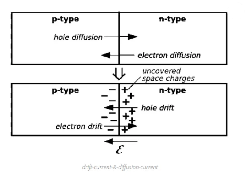
Diffusion
Diffusion refers to the movement of carriers from a region of higher concentration to a region of lower concentration, which occurs in non-uniformly doped semiconductors. This movement under gradient to attain uniformity results in diffusion current, which works to eliminate the charge gradient.
Fick's First Law
The diffusion flux is proportional to the concentration gradient:
for electrons:
for holes
Where:
D is the diffusion coefficient in m2/s
dn/dx is the concentration gradient in m-1
Therefore the diffusion Current Density will be:
for electrons:
for holes:
The total diffusion current density:
Let us suppose that the concentration of holes(p) vary with distance x
where Dp is the diffusion constant or diffusion coeficient or diffusivity of holes.
The hole concentration is higher at lower value of x, so we assume the concentration gradient is negative along the +ve x-direction and the diffusion current due to holes is +ve along the +ve x-direction.
Similarly diffusion current density for electrons
Here we take the positive sign because electronic charge is negative and also the concentration gradient is negative which makes Je2 +ve and also it is +ve along the -ve x-axis.
SO the resultant diffusion current density for both electrons and holes is
The total current density in semiconductor is the sum of drift current and diffusion current and is given by