
Extraction of bipolar SPICE Gummel-Poon parameters related to B-C junction Capacitance-Voltage (C-V) 
Theory
Introduction:
BJT B-C Junction C-V Parameter Extraction
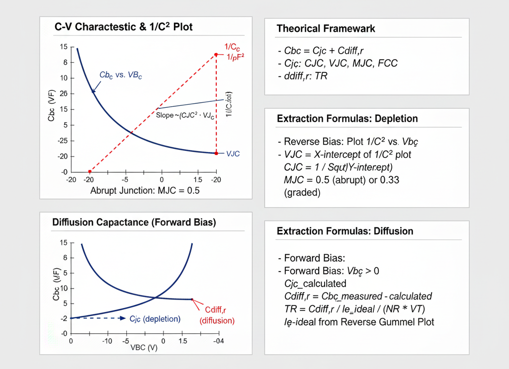
Fig. 1. BJT Base-Collector C-V Characteristics & Parameter Extraction
The base-collector (B-C) junction capacitance ($C_{bc}$) is a critical parameter in the BJT SPICE model. It models the charge stored at the collector-base junction and is a key factor in determining the high-frequency performance of the transistor (e.g., the Miller effect) and its switching speed (e.g., storage time in saturation).
This capacitance is measured by applying a varying voltage across the B-C junction and measuring the capacitance, typically while the B-E junction is held at zero bias or is reverse-biased.
Like any p-n junction, the total B-C capacitance ($C_{bc}$) has two components:
- B-C Depletion Capacitance ($C_{jc}$): Dominant when the B-C junction is reverse-biased (i.e., in the forward-active region).
- B-C Diffusion Capacitance ($C_{diff,r}$): Dominant when the B-C junction is forward-biased (i.e., in the saturation region).
$$C_{bc} = C_{jc} + C_{diff,r}$$
1. Depletion Capacitance ($C_{jc}$)
This capacitance arises from the fixed, uncovered charge in the depletion region (or space-charge region) at the B-C junction.
Key SPICE Parameters
CJC(B-C Zero-Bias Capacitance): The value of the depletion capacitance when the applied B-C voltage is zero. (Also known asCBC).VJC(B-C Built-in Potential): The built-in potential of the B-C junction (e.g., ~0.5-0.7V). (Also known asPBC).MJC(B-C Grading Coefficient): Describes the doping profile of the junction (e.g., 0.5 for abrupt, 0.33 for graded). (Also known asMC).FCC(Forward-Bias Capacitance Coefficient): A fitting parameter (default 0.5) to linearize the capacitance in the forward-bias region.
The Model Equation
The depletion capacitance under reverse bias ($V_{BC} < FCC \cdot VJC$) is modeled by the same equation as a diode:
$$C_{jc} = \frac{CJC}{(1 - V_{BC} / VJC)^{MJC}}$$
(Note: For reverse bias, $V_{BC}$ is negative, so the denominator increases and capacitance decreases.)
Extraction Method: The $1/C^2$ Plot
The parameters CJC, VJC, and MJC are extracted from C-V measurements taken while the B-C junction is reverse-biased.
The extraction method linearizes the model equation. For an abrupt junction (MJC = 0.5), which is a common approximation for the B-C junction, we plot $1/C_{jc}^2$ vs. $V_{BC}$:
$$\frac{1}{C_{jc}^2} = \frac{1 - V_{BC} / VJC}{CJC^2} = \left( \frac{1}{CJC^2} \right) - \left( \frac{1}{CJC^2 \cdot VJC} \right) \cdot V_{BC}$$
This equation is in the linear form $y = b + m \cdot x$:
- $y = 1/C_{jc}^2$
- $x = V_{BC}$ (the applied voltage)
- $b = 1/CJC^2$ (the y-intercept)
- $m = -1 / (CJC^2 \cdot VJC)$ (the slope)
Extraction Procedure:
- Measure C-V: Measure the B-C capacitance $C_{bc}$ at several reverse bias voltages $V_{BC}$ (e.g., from 0V to -20V), while $V_{BE} = 0$. In this condition, $C_{bc} \approx C_{jc}$.
- Plot Data: Create a plot of $1/C_{bc}^2$ (y-axis) versus $V_{BC}$ (x-axis). The data should form a straight line.
- Extract
VJC: Extend the straight line to the x-axis (where $y=0$). The x-intercept is the junction potential,VJC. - Extract
CJC: The y-intercept (at $V_{BC} = 0$) is $1/CJC^2$. Therefore,CJCis calculated as: $$CJC = \frac{1}{\sqrt{\text{y-intercept}}}$$ - Verify
MJC: If the plot is a straight line, the assumption thatMJC = 0.5is correct. If it is curved, a differentMJCvalue (e.g., 0.33 for a graded junction, requiring a $1/C_{bc}^3$ plot) may be needed.
2. Diffusion Capacitance ($C_{diff,r}$)
This capacitance arises from the charge of minority carriers injected into the base and collector when the B-C junction is forward-biased (i.e., when the transistor is in saturation).
Key SPICE Parameter
TR(Reverse Transit Time): Represents the mean time for carriers injected from the collector to transit through the base (in reverse-active mode).
The Model Equation
The reverse diffusion capacitance is proportional to the reverse transit time and the change in the reverse injection current:
$$C_{diff,r} = TR \cdot \frac{dI_{E,ideal}}{dV_{BC}} \approx TR \cdot \frac{I_{E,ideal}}{NR \cdot V_T}$$
Where $I_{E,ideal}$ is the ideal emitter current from the reverse Gummel plot.
Extraction Method
The reverse transit time TR is extracted from measurements taken while the B-C junction is forward-biased (i.e., in the saturation or reverse-active region).
Extraction Procedure:
- Measure $C_{bc}$ in Forward Bias: Measure the total capacitance $C_{bc}$ at one or more forward-bias $V_{BC}$ values (e.g., 0.2V, 0.3V, 0.4V).
- Calculate $C_{jc}$: At these forward-bias points, the depletion capacitance $C_{jc}$ is still present. Calculate its value using the forward-bias portion of its model (which uses the
FCCparameter). - Isolate $C_{diff,r}$: Subtract the calculated depletion capacitance from the total measured capacitance: $$C_{diff,r} = C_{bc, \text{measured}} - C_{jc, \text{calculated}}$$
- Extract
TR: Re-arrange the model equation to solve forTR. You will need the values of the ideal emitter current ($I_{E,ideal}$) from the reverse Gummel plot at the same $V_{BC}$ points. $$TR = \frac{C_{diff,r}}{(I_{E,ideal} / (NR \cdot V_T))}$$
Alternatively, TR can be extracted from high-frequency S-parameter measurements or by measuring the storage time ($t_s$) of the transistor when turning off from saturation.