Design of Arithmetic Logic Unit 
Procedure
Please follow these steps to do the experiment.
Part 1:
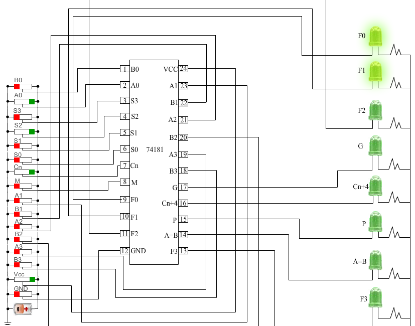
- first apply high voltage to Vcc.Then apply high voltage to M(mode control input) and low voltage to all the 4 select inputs.Logical operation will be performed.The output will be inverted A.
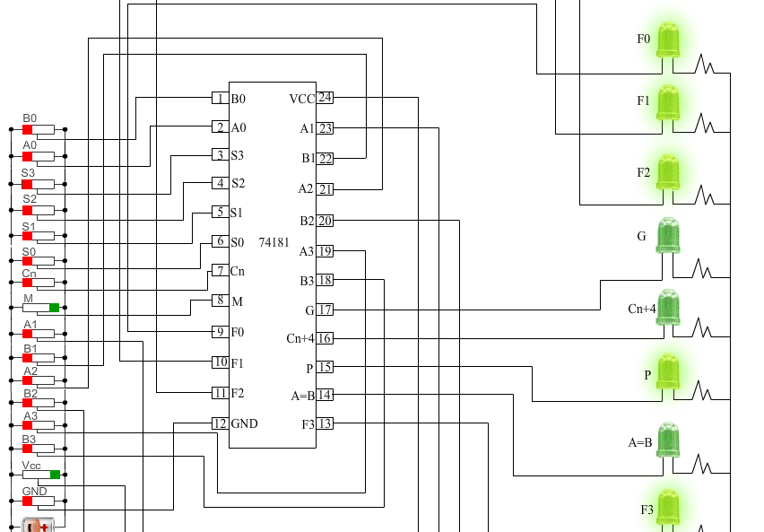
- Next, apply high voltage to S0 and apply low voltage to all other select inputs.The output will be A + B.
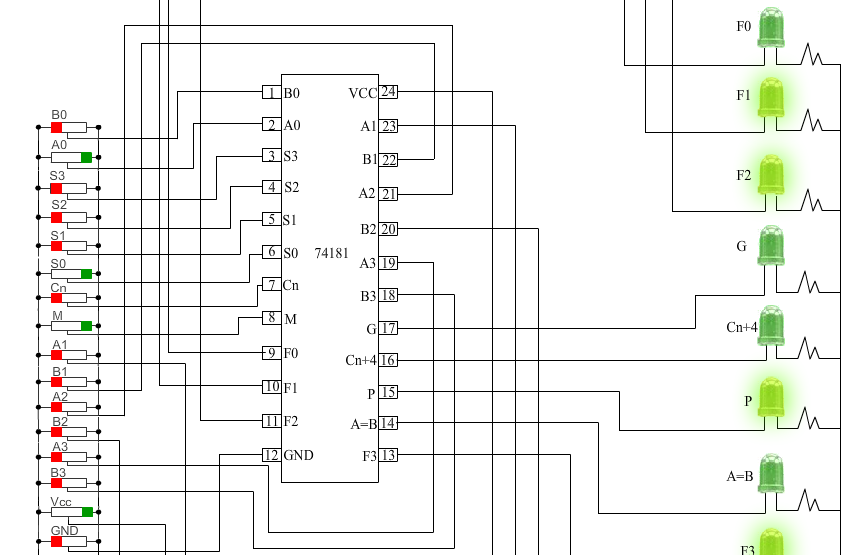
- Now apply high voltage to S1 and low voltage to all other select inputs.The output will be AB.
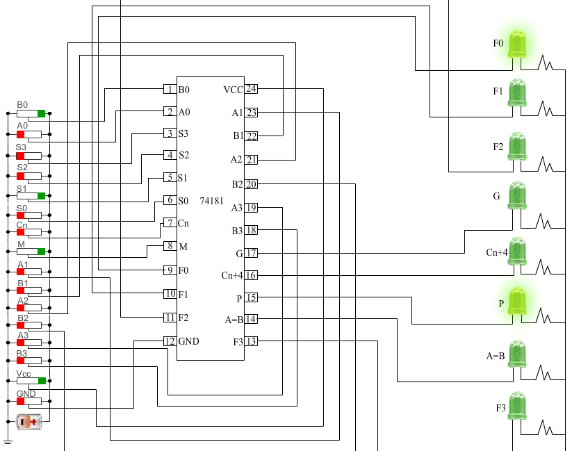
- Next, apply high voltage to S0 and S1 and low voltage to other select inputs.The output will be logical 1
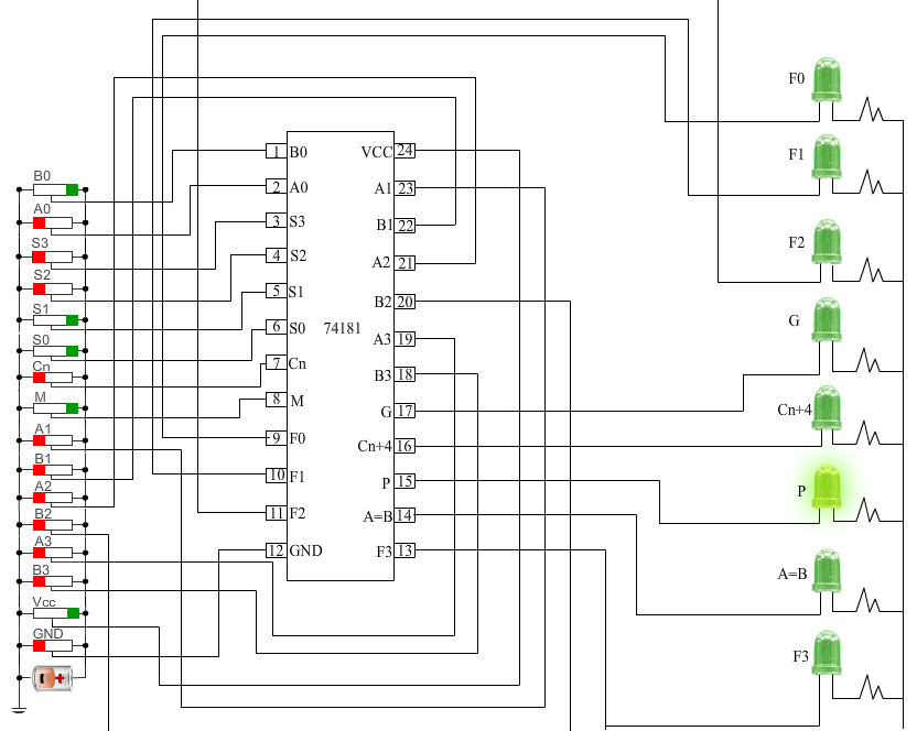
Apply high voltage to S2 and apply low voltage to all other select inputs.The output will be AB.
Apply all the combinations to all the select inputs and check the logical output.
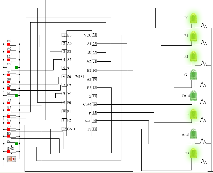
Apply low voltage to mode control input and high voltage to Cin.Now the operation mode will be arithmetic mode.
Next apply low voltages to all the select inputs.The output will be A + 1.
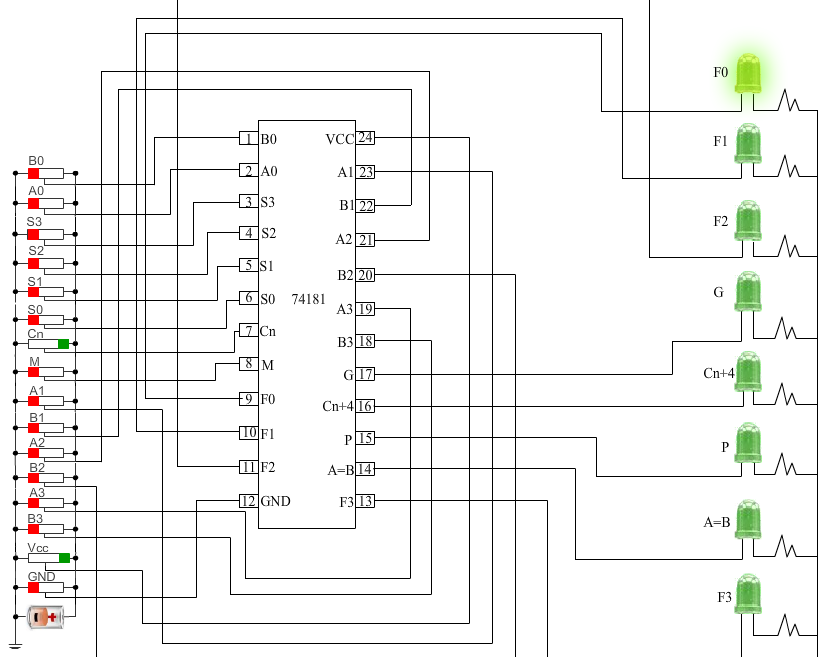
- Next, apply high voltage to S0 and low voltage to all other select inputs.The output will be A + B + 1.
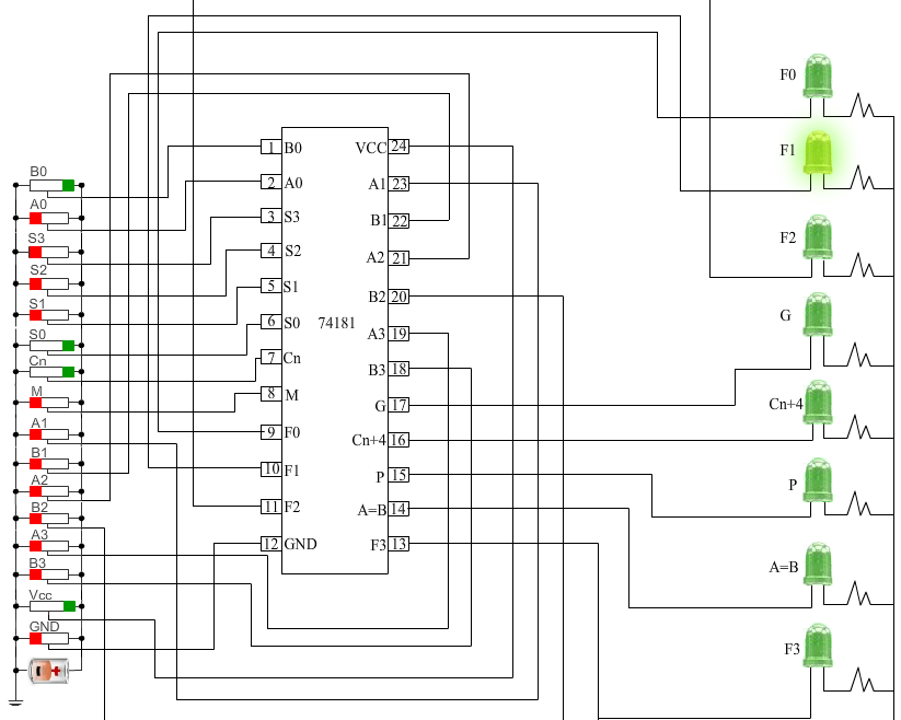
- Apply high voltage to S1 and apply low voltages to all other select inputs.The output will be A + B.
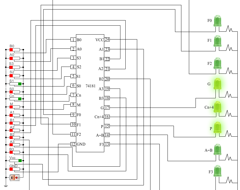
- Now apply high voltage to S0 and S1 and low volage to all other select inputs.The output will be -1 + 1.It means outputput will be zero.
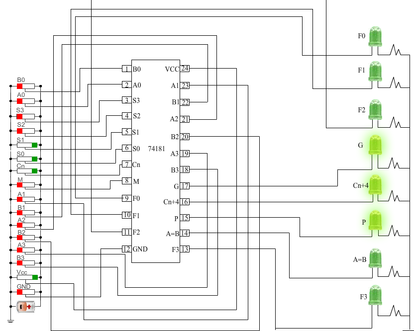
- Next, apply high voltage to S2 and low voltage to all other select inputs.The output will be A plus AB.
