
ALU with function
1-bit Programmable ALU
Circuit Diagram
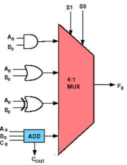
Figure 1: 1-bit Programmable ALU circuit diagram showing multiplexer-based function selection with arithmetic and logic components. Reference: Theory section
Components Required
- 1 Full Adder
- 1 AND gate
- 1 OR gate
- 1 XOR gate
- 1 4-to-1 Multiplexer
Circuit Connections
Full Adder Setup: Drag the full adder and connect inputs A₀ and B₀ to its input pins A and B respectively, and connect C₀ to its Cin input pin. This will handle the arithmetic addition operation when selected.
Logic Gates Setup: Drag AND, OR, and XOR gates and connect inputs A₀ and B₀ to their input pins. These gates will perform the logical operations when selected by the multiplexer.
Carry Output Connection: Connect the Cout (carry output) of the full adder to the Cout output bit. This provides the carry signal for arithmetic operations.
Multiplexer Configuration: Drag a 4-to-1 multiplexer and connect its select lines S₁ and S₀ to the S₁ and S₀ control bits respectively.
Multiplexer Input Connections (refer to the demo for visual guidance with labeled inputs):
- Connect I₀ of multiplexer to the "Sum" output of the full adder (for addition operation - selected when S₁S₀ = 00)
- Connect I₁ of multiplexer to the output of the AND gate (for AND operation - selected when S₁S₀ = 01)
- Connect I₂ of multiplexer to the output of the OR gate (for OR operation - selected when S₁S₀ = 10)
- Connect I₃ of multiplexer to the output of the XOR gate (for XOR operation - selected when S₁S₀ = 11)
Output Connection: Connect the output of the multiplexer to the main output bit.
Testing: Set the values of A₀, B₀, C₀, S₁, and S₀ according to your test requirements and click "Simulate".
Note: The demo visualization includes enhanced MUX input labels (I₀(00), I₁(01), I₂(10), I₃(11)) with colored backgrounds to help you understand which operation is selected by each S₁S₀ combination.
ALU Function Table
| S₁ | S₀ | Operation | Description |
|---|---|---|---|
| 0 | 0 | Addition | Output = A₀ + B₀ + C₀ (with carry) |
| 0 | 1 | AND | Output = A₀ · B₀ |
| 1 | 0 | OR | Output = A₀ + B₀ |
| 1 | 1 | XOR | Output = A₀ ⊕ B₀ |
Testing Procedures
Addition Operation (S₁S₀ = 00):
- Set S₁ = 0, S₀ = 0 to select addition mode
- Test various combinations of A₀, B₀, and C₀ inputs
- Observe both Sum output and Carry output (Cout)
- Verify results match full adder truth table
Logic Operations (S₁S₀ = 01, 10, 11):
- Set appropriate S₁S₀ combinations for AND, OR, or XOR operations
- Test with different A₀ and B₀ input combinations
- Observe output matches the selected logical operation
- Note that C₀ input is not used for logic operations
Observations
Function Selection: The multiplexer selects which operation result appears at the output based on S₁S₀ control signals, as described in the theory section. The demo visualization shows labeled MUX inputs (I₀(00), I₁(01), I₂(10), I₃(11)) to clarify this selection process.
Arithmetic Mode: When S₁S₀ = 00, the ALU performs addition of A₀, B₀, and C₀, producing both Sum and Carry outputs for potential cascading to higher-order bits.
Logic Modes: When S₁S₀ = 01, 10, or 11, the ALU performs AND, OR, or XOR operations respectively, with the Carry output being irrelevant for these operations.
Control Signal Behavior: The S₁S₀ control signals act as a simple instruction set, determining which arithmetic or logical operation the ALU executes.
Visual Learning Aid: The enhanced demo includes colored background labels for MUX inputs, making it easier to understand the relationship between control signals and selected operations.
Success Verification: If the circuit has been constructed correctly as described above, a "Success" message will be displayed upon clicking the "Submit" button.
Circuit Building Guidelines
Component Placement: Arrange components logically with inputs on the left, processing elements in the middle, and outputs on the right for clear signal flow visualization.
Wire Management: Use clean, direct connections between components to avoid crossing wires and maintain circuit readability.
Input Testing: Systematically test all possible input combinations for each operation mode to verify correct ALU functionality.
Signal Verification: Double-check that control signals S₁S₀ properly select the intended operation by observing output changes when switching between functions.
Troubleshooting
Incorrect Outputs: Verify that multiplexer inputs are connected to the correct operation outputs (I₀→Sum, I₁→AND, I₂→OR, I₃→XOR). Use the demo's visual labels as a reference.
Function Selection Issues: Check that S₁ and S₀ control lines are properly connected to the multiplexer select inputs. The demo shows how each S₁S₀ combination (00, 01, 10, 11) corresponds to specific MUX inputs.
Carry Problems: Ensure the full adder's Cout is connected to the ALU's Carry output for arithmetic operations.
Logic Operation Errors: Verify that A₀ and B₀ inputs are correctly connected to all logic gates (AND, OR, XOR) as well as the full adder.
Demo Reference: Use the enhanced demo visualization with colored MUX input labels to verify your circuit connections match the intended design.