
Frequency Modulation
Theory :
Frequency modulation (FM) is the process where the frequency of a carrier wave, denoted as \( c(t) \), is varied in accordance with the instantaneous amplitude of the modulating signal \( m(t) \). Unlike amplitude modulation, where the amplitude of the carrier wave is varied, in FM, the amplitude remains constant while the frequency changes. The modulated signal can be mathematically expressed as:
\( S(t) = A_c \cos\left[ 2\pi f_c t + 2\pi K_f \int m(\tau) d\tau \right] \)
Where:
- \( A_c \) is the amplitude of the carrier signal.
- \( f_c \) is the carrier frequency.
- \( K_f \) is the frequency sensitivity of the modulator, defining how much the frequency of the carrier varies with the modulating signal.
- \( m(t) \) is the modulating (baseband) signal.
- \( \int m(\tau) d\tau \) represents the integral of the modulating signal, which determines the frequency deviation.
This expression shows that the instantaneous frequency of the carrier wave is proportional to the amplitude of the modulating signal. The carrier frequency \( f_c \) is shifted by an amount proportional to the modulating signal \( m(t) \), and this shift results in a frequency-modulated signal.
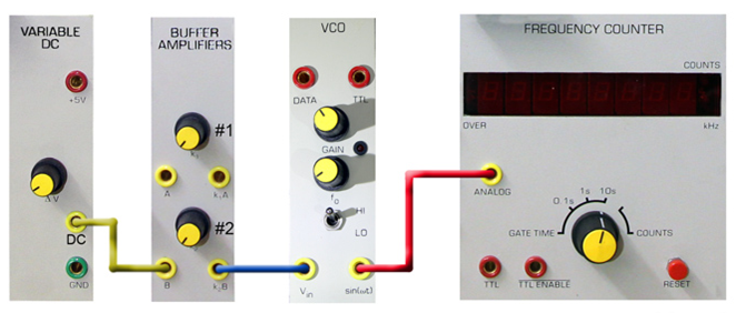
Block Diagram
Procedures:
We use a voltage-controlled oscillator (VCO) as an FM modulator. The
VCO’s input voltage, V𝑖 , determines the VCO’s output signal
frequency as:
𝑓out = 𝑓center + 𝑘𝑓V𝑖n
Where, 𝑓center is the carrier frequency, kf is the sensitivity of
the frequency modulator (here, VCO), and Vin is the voltage of
message signal
In this frequency modulation, we study the impact of the amplitude
and frequency of the message signal on FM signals.
In the ‘VCO’ module, the frequency range switch selects between
the HI or carrier band and the LO or audio band.
1. Set the VCO module’s on-board
mode switch to “VCO” and the VCO front panel’s switch to “LO.” Set
the VCO front panel gain control fully counter-clockwise (so that
the VCO input, Vin, has no effect on the VCO’s output frequency).
2. In order to set the
sensitivity factor of the FM modulator, you need to use the variable
DC module and the buffer amplifier on the TIMS front panel. Set the
variable DC gain control fully counter-clockwise. Connect the output
of variable DC module to the input of buffer amplifier and adjust it
to make a 1V DC signal. Connect this 1V DC signal to the input of
the VCO as shown in Figure 1.
3. Adjust the VCO front panel f0
control to set the center frequency to 10 kHz. (for selecting
carrier frequency switch to ‘HI’ in the ‘VCO’ module). Now adjust
the VCO gain control until the VCO’s output frequency changes by 1
kHz. This means that 𝑘𝑓 is set to 1 KHz/volt . (Note that due to the
VCO’s internal settings, you will see a 1 kHz decrease with respect
to the center frequency.)
4. Disconnect the DC signal from
the VCO and instead, connect a 2V p-p 500 Hz sinusoidal signal to
the VCO. You can use the AUDIO OSCILLATOR module and buffer
amplifier to make a 2V p-p 500 Hz sinusoidal signal. Observe the FM
signal on the Oscilloscope. Take screen shot from the Oscilloscope
and attach to your report.
What are the minimum and maximum frequencies observed on the
Oscilloscope?
What is the corresponding modulation index?
[Hint: On the Oscilloscope, you should observe the Maximum and
minimum frequencies]
5. Change the message amplitude
to 3V p-p. What are the minimum and maximum frequencies observed on
the Oscilloscope? What is the corresponding modulation index?
6. Now change the frequency
sensitivity factor of the FM modulator to 2KHz/volt. Repeat steps 4
and 5 for the new frequency sensitivity factor
Frequency Demodulation
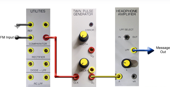
Block Diagram
Procedures:
1. A simple FM demodulator, if
it reproduces the message without distortion, will provide further
confirmation that the VCO output is indeed an FM signal. The
zero-crossing counter is shown in figure 2. A simple yet effective
FM demodulator is one which takes a time average of the zero
crossings of the FM signal.
2. This signal COMPARATOR with
TTL output and CLIPPER with bipolar output, for squaring analog
waveforms. ‘UTILITIES- COMPARATOR’s threshold level may be set as
required by applying a DC voltage to the REF input
3. The ‘TWIN PULSE GENERATOR’ in
SINGLE mode, only Q1 outputs a positive going pulse, while Q2
outputs the inverse of Q1. The pulse width can be varied.
4. The TWIN PULSE GENERATOR is
required to produce a pulse at each positive going zero crossing of
the FM signal. To achieve this, the FM signal is converted to a TTL
signal by the COMPARATOR, and this drives the TWIN PULSE GENERATOR.
5. Note: the input signal to the
HEADPHONE AMPLIFIER filter (LPF, cut-off frequency – 3 KHz) is at
TTL level. It is TIMS practice, in order to avoid overload, not to
connect a TTL signal to an analog input. Check for overload. If you
prefer you can use the yellow analog output from the TWIN PULSE
GENERATOR. This is an AC coupled version of the TTL signal.
6. Before plugging in the TWIN
PULSE GENERATOR set the on-board MODE switch SW1 to SINGLE. Patch up
the demodulator of figure 2.
7. Set the frequency deviation
of the FM generator to zero, and connect the VCO output to the
demodulator input.
8. Using the WIDTH control of
the TWIN PULSE GENERATOR adjust the output pulses to their maximum
width.
9. Observe the demodulator
output. If you have chosen to take the TTL output from the TWIN
PULSE GENERATOR there should be a DC voltage present. Why? Notice
that it is proportional to the width of the pulses into the LPF of
the HEADPHONE AMPLIFIER.
10. Introduce some modulation at
the VCO with the BUFFER amplifier gain control. Observe the
demodulated output from the LPF of the HEADPHONE AMPLIFIER using the
oscilloscope. Measure its frequency (and compare with the message
source at the transmitter).