

Odd Parity Generator
1
7
14
8
1
7
14
8
P
A
C
+ -
A
B
C
Check Connections
Start Simulation
Reset Connections
Instructions
Components
✕
Fill the truth table and click on
'CHECK'
button.
Click on the components button to place the component.
Make connections as per the circuit diagram.
Fig. 1 Circuit diagram of odd parity generator.
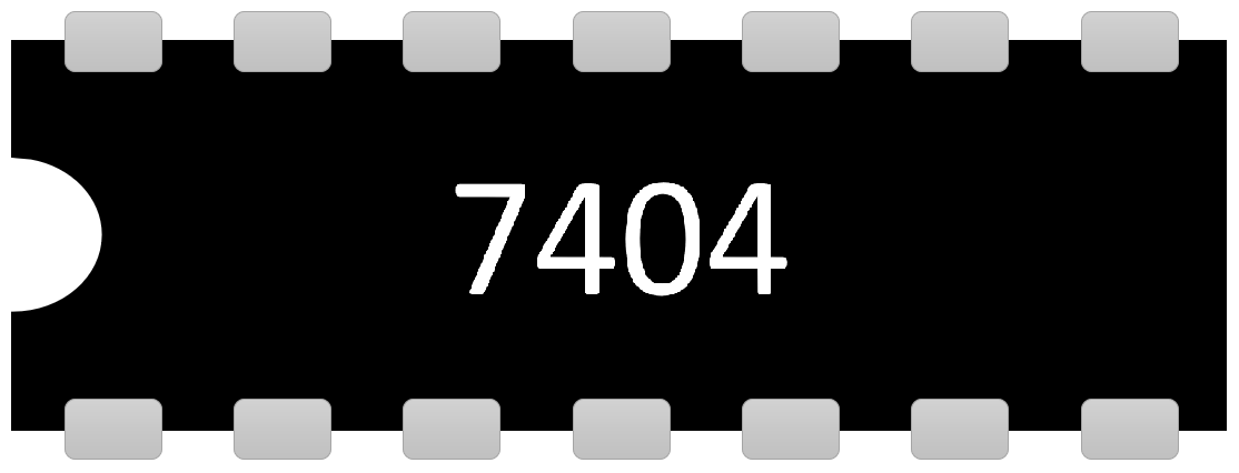
Fig: 2 Pin diagram of IC-7486 and IC-7404.
Feed input
A
and
B
to one gate of IC and input
C
to another gate.
Click on '
Check Connections
' button. If connections are right, the '
Start Simulation
' button will become active. Click on it to start simulation.
Click on the toggle buttons '
A
', '
B
' and '
C
' to perform simulation.
✕
Breadboard
5V DC Supply
Toggle Switches
IC-7486
IC-7404
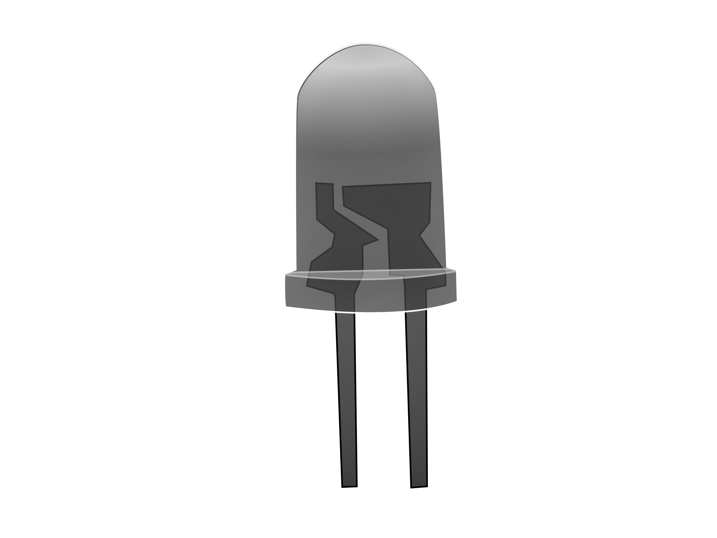
LED
TRUTH TABLE
Components button will remain inactive until Truth-Table is filled correctly.
INPUTS A B C
PARITY BIT P
0 0 0
0 0 1
0 1 0
0 1 1
1 0 0
1 0 1
1 1 0
1 1 1
CHECK
RESET